Closed Dec 25th-26th
800-300-1968
We Stock Hard to Find Parts
My Account
|
My Orders
|
My Cart
Questions?
(800) 300-1968
Register
(current)
My Account
(current)
My Orders
(current)
My Cart
(current)
Categories
(current)
Manufacturers
Request a Quote
Sell Your Excess
Consignment
Quality Assurance
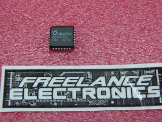
SY10EL15ZC
Part #
SY10EL15ZC
Description
IC CLK BUFFER 2:4 16SOIC
Category
IC
Availability
In Stock
Qty
5
Qty
Price
1 +
$4.12032
Manufacturer
Available
Qty
Micrel
Date Code: 0124
Freelance Stock:
5
Ships Immediately
Add to Cart
Related Items
SYNERGY
IC
SY10E104JC
$4.22730
SYNERGY
IC
SY10E111JC
$5.06274
SYNERGY
IC
SY10E136JC
$16.30584
SYNERGY
IC
SY10E143JC
$9.23747
SYNERGY
IC
SY10E404JC
$9.94463
SYNERGY
IC
SY10E452JC
$16.30584