Closed Dec 25th-26th
800-300-1968
We Stock Hard to Find Parts
My Account
|
My Orders
|
My Cart
Questions?
(800) 300-1968
Register
(current)
My Account
(current)
My Orders
(current)
My Cart
(current)
Categories
(current)
Manufacturers
Request a Quote
Sell Your Excess
Consignment
Quality Assurance
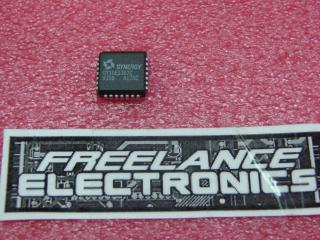
SY10E104JC
Part #
SY10E104JC
Description
IC GATE AND/NAND QUINT 28-PLCC
Category
IC
Availability
Out of Stock
Qty
0
Qty
Price
1 +
$3.20250
Related Items
Generic
IC
SY10E111JC
$3.83541
Generic
IC
SY10E136JC
$12.35291
Generic
IC
SY10E143JC
$6.99808
Generic
IC
SY10E404JC
$7.53381
Generic
IC
SY10E452JC
$12.35291
Generic
IC
SY10EL15ZC
$4.12032