MSP430x22x2, MSP430x22x4
MIXED SIGNAL MICROCONTROLLER
SLAS504B − JULY 2006 − REVISED JULY 2007
32
POST OFFICE BOX 655303 • DALLAS, TEXAS 75265
POST OFFICE BOX 1443 • HOUSTON, TEXAS 77251−1443
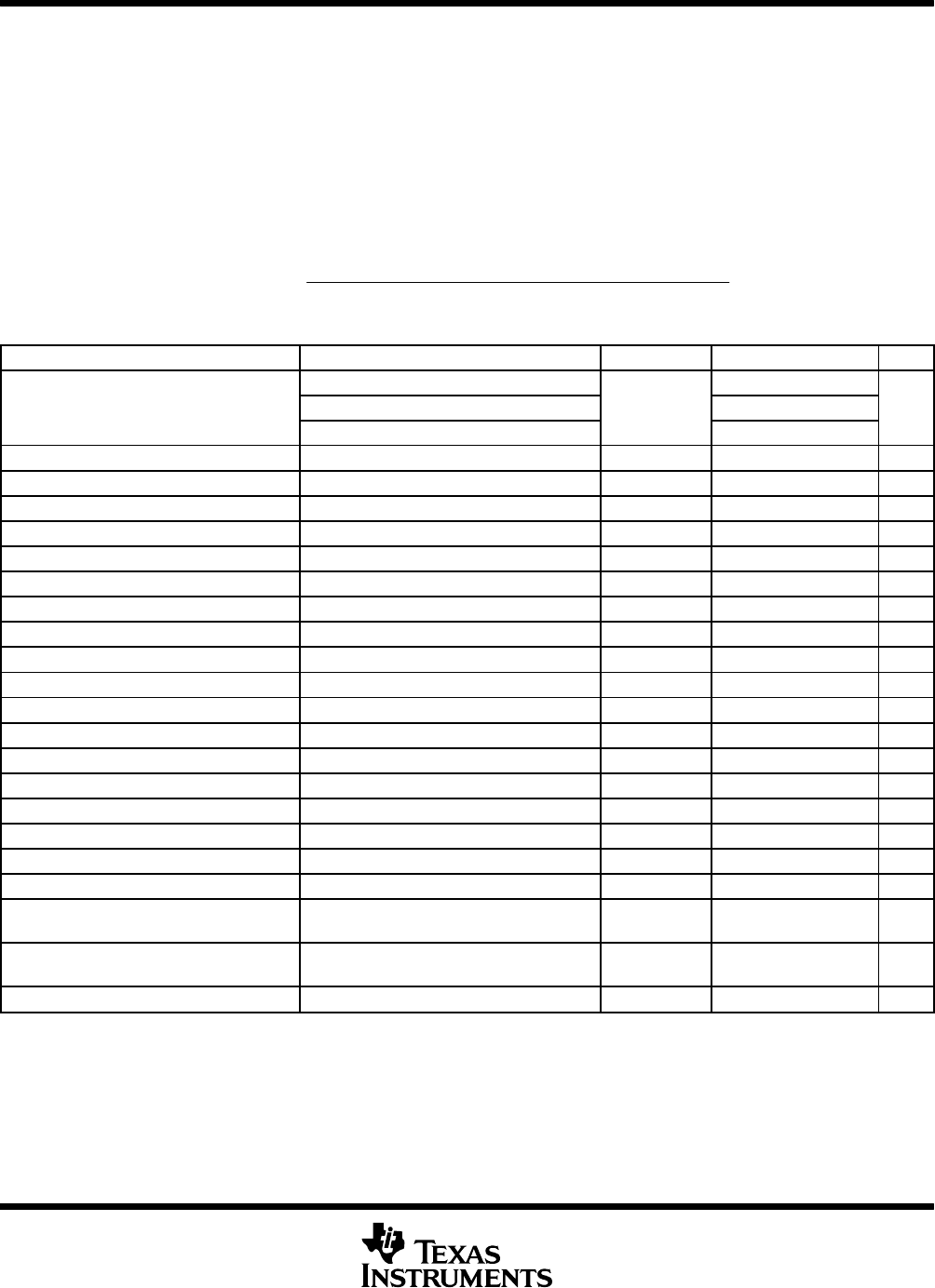
electrical characteristics over recommended ranges of supply voltage and operating free-air
temperature (unless otherwise noted) (continued)
main DCO characteristics
D All ranges selected by RSELx overlap with RSELx + 1: RSELx = 0 overlaps RSELx = 1, ... RSELx = 14
overlaps RSELx = 15.
D DCO control bits DCOx have a step size as defined by parameter S
DCO
.
D Modulation control bits MODx select how often f
DCO(RSEL,DCO+1)
is used within the period of 32 DCOCLK
cycles. The frequency f
DCO(RSEL,DCO)
is used for the remaining cycles. The frequency is an average equal
to:
f
average
+
32 f
DCO(RSEL,DCO)
f
DCO(RSEL,DCO)1)
MOD f
DCO(RSEL,DCO)
)(32*MOD) f
DCO(RSEL,DCO)1)
DCO frequency
PARAMETER TEST CONDITIONS VCC MIN TYP MAX UNIT
RSELx < 14 1.8 3.6
Vcc Supply voltage range
RSELx = 14 2.2 3.6
V
RSELx = 15 3.0 3.6
f
DCO(0,0)
DCO frequency (0, 0) RSELx = 0, DCOx = 0, MODx = 0 2.2 V/3 V 0.06 0.14 MHz
f
DCO(0,3)
DCO frequency (0, 3) RSELx = 0, DCOx = 3, MODx = 0 2.2 V/3 V 0.07 0.17 MHz
f
DCO(1,3)
DCO frequency (1, 3) RSELx = 1, DCOx = 3, MODx = 0 2.2 V/3 V 0.10 0.20 MHz
f
DCO(2,3)
DCO frequency (2, 3) RSELx = 2, DCOx = 3, MODx = 0 2.2 V/3 V 0.14 0.28 MHz
f
DCO(3,3)
DCO frequency (3, 3) RSELx = 3, DCOx = 3, MODx = 0 2.2 V/3 V 0.20 0.40 MHz
f
DCO(4,3)
DCO frequency (4, 3) RSELx = 4, DCOx = 3, MODx = 0 2.2 V/3 V 0.28 0.54 MHz
f
DCO(5,3)
DCO frequency (5, 3) RSELx = 5, DCOx = 3, MODx = 0 2.2 V/3 V 0.39 0.77 MHz
f
DCO(6,3)
DCO frequency (6, 3) RSELx = 6, DCOx = 3, MODx = 0 2.2 V/3 V 0.54 1.06 MHz
f
DCO(7,3)
DCO frequency (7, 3) RSELx = 7, DCOx = 3, MODx = 0 2.2 V/3 V 0.80 1.50 MHz
f
DCO(8,3)
DCO frequency (8, 3) RSELx = 8, DCOx = 3, MODx = 0 2.2 V/3 V 1.10 2.10 MHz
f
DCO(9,3)
DCO frequency (9, 3) RSELx = 9, DCOx = 3, MODx = 0 2.2 V/3 V 1.60 3.00 MHz
f
DCO(10,3)
DCO frequency (10, 3) RSELx = 10, DCOx = 3, MODx = 0 2.2 V/3 V 2.50 4.30 MHz
f
DCO(11,3)
DCO frequency (11, 3) RSELx = 11, DCOx = 3, MODx = 0 2.2 V/3 V 3.00 5.50 MHz
f
DCO(12,3)
DCO frequency (12, 3) RSELx = 12, DCOx = 3, MODx = 0 2.2 V/3 V 4.30 7.30 MHz
f
DCO(13,3)
DCO frequency (13, 3) RSELx = 13, DCOx = 3, MODx = 0 2.2 V/3 V 6.00 9.60 MHz
f
DCO(14,3)
DCO frequency (14, 3) RSELx = 14, DCOx = 3, MODx = 0 2.2 V/3 V 8.60 13.9 MHz
f
DCO(15,3)
DCO frequency (15, 3) RSELx = 15, DCOx = 3, MODx = 0 3 V 12.0 18.5 MHz
f
DCO(15,7)
DCO frequency (15, 7) RSELx = 15, DCOx = 7, MODx = 0 3 V 16.0 26.0 MHz
S
RSEL
Frequency step between
range RSEL and RSEL+1
S
RSEL
= f
DCO(RSEL+1,DCO)
/f
DCO(RSEL,DCO)
2.2 V/3 V 1.55 ratio
S
DCO
Frequency step between
tap DCO and DCO+1
S
DCO
= f
DCO(RSEL,DCO+1)
/f
DCO(RSEL,DCO)
2.2 V/3 V 1.05 1.08 1.12 ratio
Duty Cycle Measured at P1.4/SMCLK 2.2 V/3 V 40 50 60 %


