Closed Dec 25th-26th
800-300-1968
We Stock Hard to Find Parts
My Account
|
My Orders
|
My Cart
Questions?
(800) 300-1968
Register
(current)
My Account
(current)
My Orders
(current)
My Cart
(current)
Categories
(current)
Manufacturers
Request a Quote
Sell Your Excess
Consignment
Quality Assurance
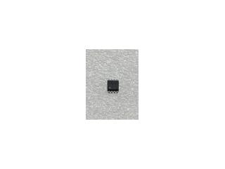
AT45DB321D-MU
Part #
AT45DB321D-MU
Description
FLASH, 32MB, DFN-8, Memory Size:32Mbit, Flash Memory Confi
Category
IC
Availability
Out of Stock
Qty
0
Qty
Price
1 +
$2.30280
Related Items
Atmel
IC
AT45DB011-SI
$11.93931
Atmel
IC
AT45DB011B-SI
$3.03764
Atmel
IC
AT45DB011D-SH-T
$2.18563
Atmel
IC
AT45DB021B-SC
$1.68757
Atmel
IC
AT45DB041B-SC-2.5
$3.77388
Atmel
IC
AT45DB081B-TC
$12.26240