AD8361
–3–
REV. A
ABSOLUTE MAXIMUM RATINGS
1
Supply Voltage V
S
. . . . . . . . . . . . . . . . . . . . . . . . . . . . . 5.5 V
SREF, PWDN . . . . . . . . . . . . . . . . . . . . . . . . . . . . . . . 0 V, V
S
IREF . . . . . . . . . . . . . . . . . . . . . . . . . . . . . . . . . V
S
– 0.3 V, V
S
RFIN . . . . . . . . . . . . . . . . . . . . . . . . . . . . . . . . . . . . . . 1 V rms
Equivalent Power re 50 Ω . . . . . . . . . . . . . . . . . . . 13 dBm
Internal Power Dissipation
2
. . . . . . . . . . . . . . . . . . . . 200 mW
SOT-23-6L . . . . . . . . . . . . . . . . . . . . . . . . . . . . . . 170 mW
micro_SOIC . . . . . . . . . . . . . . . . . . . . . . . . . . . . . . 200 mW
Maximum Junction Temperature . . . . . . . . . . . . . . . . . 125°C
Operating Temperature Range . . . . . . . . . . . –40°C to +85°C
Storage Temperature Range . . . . . . . . . . . . –65°C to +150°C
Lead Temperature Range (Soldering 60 sec) . . . . . . . . . 300°C
NOTES
1
Stresses above those listed under Absolute Maximum Ratings may cause perma-
nent damage to the device. This is a stress rating only; functional operation of the
device at these or any other conditions above those indicated in the operational
section of this specification is not implied. Exposure to absolute maximum rating
conditions for extended periods may affect device reliability.
2
Specification is for the device in free air.
SOT-23-6L: θ
JA
= 230°C/W; θ
JC
= 92°C/W.
micro_SOIC: θ
JA
= 200°C/W; θ
JC
= 44°C/W.
CAUTION
ESD (electrostatic discharge) sensitive device. Electrostatic charges as high as 4000 V readily
accumulate on the human body and test equipment and can discharge without detection. Although
the AD8361 features proprietary ESD protection circuitry, permanent damage may occur on
devices subjected to high-energy electrostatic discharges. Therefore, proper ESD precautions are
recommended to avoid performance degradation or loss of functionality.
PIN FUNCTION DESCRIPTIONS
Pin
Micro SOT Name Description
1 6 VPOS Supply Voltage Pin. Operational range
2.7 V to 5.5 V.
2 IREF Output Reference Control Pin. Inter-
nal reference mode enabled when pin
is left open. Otherwise, this pin should
be tied to VPOS. DO NOT ground this
pin.
3 5 RFIN Signal Input Pin. Must be driven from
an ac-coupled source. The low frequency
real input impedance is 225 Ω.
4 4 PWDN Power-Down Pin. For the device to
operate as a detector it needs a logical
low input (less than 100 mV). When
a logic high (greater than V
S
– 0.5 V)
is applied, the device is turned off and
the supply current goes to nearly zero
(ground and internal reference mode
less than 1 µA, supply reference mode
V
S
divided by 100 kΩ).
5 2 COMM Device Ground Pin.
6 3 FLTR By placing a capacitor between this pin
and VPOS, the corner frequency of the
modulation filter is lowered. The on-
chip filter is formed with 27 pF储2 kΩ
for small input signals.
7 1 VRMS Output Pin. Near-rail-to-rail voltage
output with limited current drive capa-
bilities. Expected load >10 kΩ to ground.
8 SREF Supply Reference Control Pin. To en-
able supply reference mode this pin
must be connected to VPOS, other-
wise it should be connected to COMM
(ground).
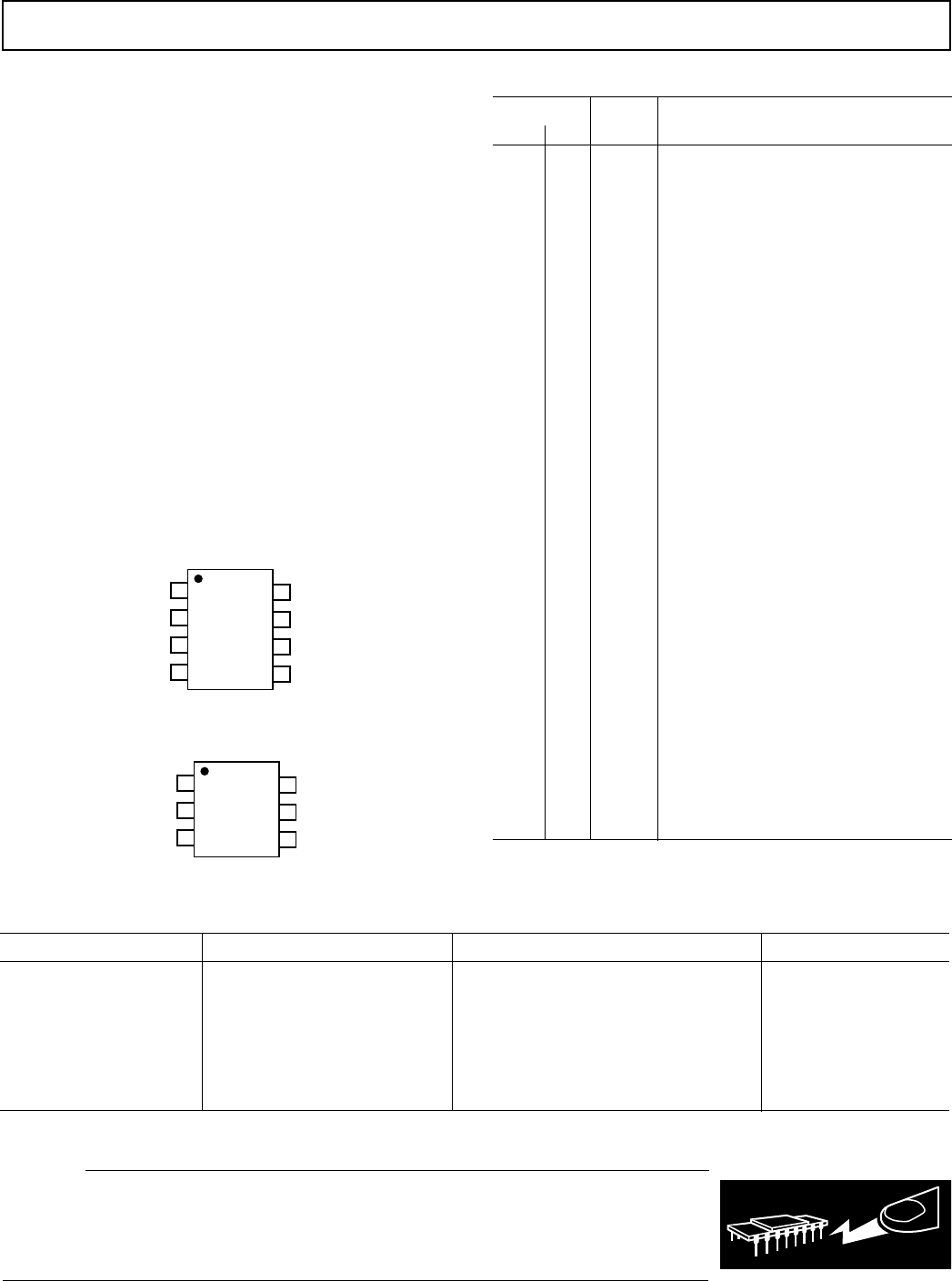
PIN CONFIGURATIONS
micro_SOIC
AD8361
VPOS
IREF
RFIN
PWDN
SREF
VRMS
FLTR
COMM
1
2
3
4
5
6
7
8
SOT-23-6L
VPOS
RFIN
PWDN
VRMS
FLTR
COMM
1
2
3
4
5
6
AD8361
ORDERING GUIDE
Model Temperature Range Package Description Package Option
AD8361ARM* –40°C to +85°C Tube, 8-Lead micro_SOIC RM-8
AD8361ARM-REEL 13" Tape and Reel
AD8361ARM-REEL7 7" Tape and Reel
AD8361ART-REEL 13" Tape and Reel RT-6
AD8361ART-REEL7 7" Tape and Reel
AD8361-EVAL Evaluation Board micro_SOIC
AD8361ART-EVAL Evaluation Board SOT-23-6L
*Device branded as J3A.
WARNING!
ESD SENSITIVE DEVICE