Closed Dec 25th-26th
800-300-1968
We Stock Hard to Find Parts
My Account
|
My Orders
|
My Cart
Questions?
(800) 300-1968
Register
(current)
My Account
(current)
My Orders
(current)
My Cart
(current)
Categories
(current)
Manufacturers
Request a Quote
Sell Your Excess
Consignment
Quality Assurance
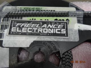
AD8361ARMZ
Part #
AD8361ARMZ
Description
MINSO DC-2.5GHZ TRUE PWR DETECTOR/CNTRLR
Category
IC
Availability
In Stock
Qty
15
Qty
Price
1 - 3
$6.08941
4 - 6
$4.84385
7 - 9
$4.56706
10 - 12
$4.24413
13 +
$3.78282
Manufacturer
Available
Qty
Analog Devices
Date Code: 1122
Freelance Stock:
15
Ships Immediately
Add to Cart
Related Items
Analog Devices
IC
AD8361-ARM
$16.07215
Analog Devices
IC
AD8361ARM
$8.75163
Analog Devices
IC
AD8361ART
$9.01016
Analog Devices
IC
AD8361ART-REEL7
$6.71414
Analog Devices
IC
AD8367ARU
$6.13250
Generic
IC
AD8367ARU-REEL7
$16.58646