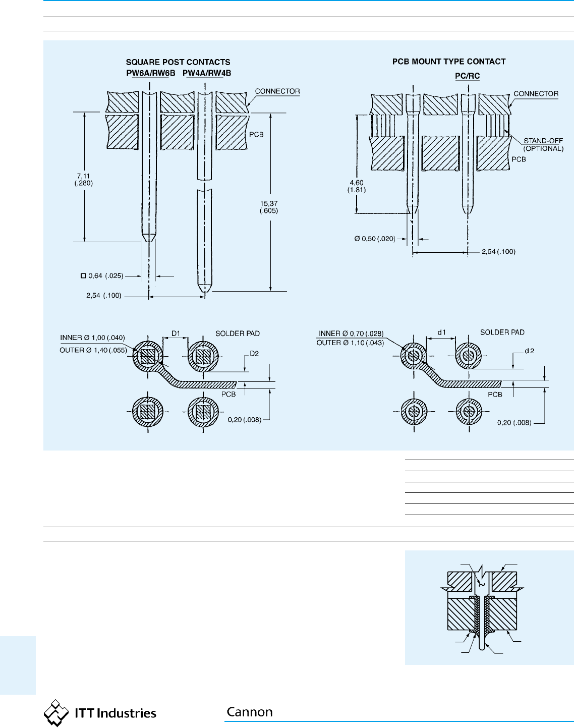
Dimensions are shown in mm (inch)
Dimensions subject to change
64
Reader’s
Resource
ZIF Connectors DL/DLM/DLD
PCB Pad Layout
For the PC/RC Versions; The contact tail design
has been modified from a 0,64 (.025) square pin to
a 0,05 (.020) diameter round pin. The change
enables a decrease in the diameter of the through-
holes as well as the solder mounds on PCB’s (d1,
and d2 can be wider than D1 and D2). This can
reduce the crosstalk in RF circuits and enhance the
dielectric withstanding voltage in high voltage
circuits.
Dimensions
D1 1,14 (.045)
D2 0,47 (.018)
d1 1,44 (.057)
d2 0,62 (.024)
PCB Pad Layout
The soldering of contacts into through (THRU)
holes on a PC Board has become standard for
medical equipment and test equipment for semi-
conductors. As a result of the narrow spacing
between the solder pad and circuit pattern,
crosstalk between signals increases. A solution to
this problem is to make the diameter of the
contacts and solder lands smaller to provide more
space between the lands and the patterns.
However, a smaller diameter contact results in
higher impedance.
Cannon designed a solution with a smaller
diameter contact tail. This design application
allows the use of a smaller through-hole diameter.
CONTACT
SOLDER
THRU HOLE
PC TAIL
PCB
CONNECTOR
INSULATOR


