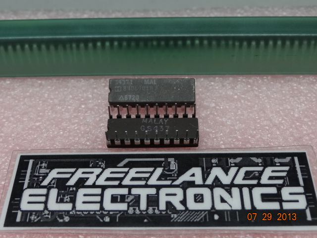
Freelance Electronics Components Distributor
Closed Dec 25th-26th
800-300-1968
We Stock Hard to Find Parts

8406701RA

Part # 8406701RA
Description CMOS OCTAL LATCHING BUS DRIVE20CDIP - Rail/Tube
Category Microcircuit
Availability In Stock
Qty 95
Qty Price
1 - 1 $157.96633
2 - 3 $125.65503
4 - 8 $118.47475
9 - 18 $110.09774
19 + $98.13060
Manufacturer Available Qty
Harris Corporation
Date Code: 9131
  • Shipping Freelance Stock: 3
    Ships Immediately
Harris Corporation
Date Code: 8714
  • Shipping Freelance Stock: 2
    Ships Immediately
Harris Corporation
Date Code: 8700
  • Shipping Freelance Stock: 90
    Ships Immediately


Technical Document


DISCLAIMER: The information provided herein is solely for informational purposes. Customers must be aware of the suitability of this product for their application, and consider that variable factors such as Manufacturer, Product Category, Date Codes, Pictures and Descriptions may differ from available inventory.

4-274
March 1997
82C82
CMOS Octal Latching Bus Driver
Features
Full Eight-Bit Parallel Latching Buffer
Bipolar 8282 Compatible
Three-State Noninverting Outputs
Propagation Delay . . . . . . . . . . . . . . . . . . . . . 35ns Max.
Gated Inputs:
- Reduce Operating Power
- Eliminate the Need for Pull-Up Resistors
Single 5V Power Supply
Low Power Operation . . . . . . . . . . . . . . . ICCSB = 10µA
Operating Temperature Ranges
- C82C82 . . . . . . . . . . . . . . . . . . . . . . . . . .0
o
C to +70
o
C
- I82C82 . . . . . . . . . . . . . . . . . . . . . . . . . -40
o
C to +85
o
C
- M82C82 . . . . . . . . . . . . . . . . . . . . . . . -55
o
C to +125
o
C
Description
The Intersil 82C82 is a high performance CMOS Octal
Latching Buffer manufactured using a self-aligned silicon
gate CMOS process (Scaled SAJI IV). The 82C82 provides
an eight-bit parallel latch/buffer in a 20 pin package. The
active high strobe (STB) input allows transparent transfer of
data and latches data on the negative transition of this sig-
nal. The active low output enable (
OE) permits simple inter-
face to state-of-the-art microprocessor systems.
Ordering Information
PART NUMBER TEMP. RANGE PACKAGE PKG. NO.
CP82C82 0
o
C to +70
o
C 20 Ld PDIP E20.3
IP82C82 -40
o
C to +85
o
C
CS82C82 0
o
C to +70
o
C 20 Ld PLCC N20.35
IS82C82 -40
o
C to +85
o
C
CD82C82 0
o
C to +70
o
C 20 Ld CERDIP F20.3
ID82C82 -40
o
C to +85
o
C
MD82C82/B -55
o
C to +125
o
C
8406701RA SMD #
MR82C82/B -55
o
C to +125
o
C 20 Pad CLCC J20.A
84067012A SMD #
Pinouts
82C82 (PDIP, CERDIP)
TOP VIEW
82C82 (PLCC, CLCC)
TOP VIEW
11
12
13
14
15
16
17
18
20
19
10
9
8
7
6
5
4
3
2
1
DI
0
DI
1
DI
2
DI
3
DI
4
DI
5
DI
7
DI
6
OE
GND
V
CC
DO
1
DO
2
DO
3
DO
0
DO
4
DO
5
DO
6
DO
7
STB
193 2 201
15
16
17
18
14
9
10 11 12 13
4
5
6
7
8
DI
4
DI
5
DI
6
DI
7
DI
3
OE
GND
STB
DO
7
DO
6
DO
2
DO
3
DO
4
DO
5
DO
1
DI
2
DI
1
DI
0
V
CC
DO
0
TRUTH TABLE
STB OE DI DO
X H X Hi-Z
HLLL
HLHH
LX
H = Logic One
L = Logic Zero
X = Don’t Care
= Latched to Value of Last
Data
Hi-Z = High Impedance
= Neg. Transition
PIN NAMES
PIN DESCRIPTION
DI
0
-DI
7
Data Input Pins
DO
0
-DO
7
Data Output Pins
STB Active High Strobe
OE Active Low Output
Enable
File Number 2975.1
CAUTION: These devices are sensitive to electrostatic discharge; follow proper IC Handling Procedures.
http://www.intersil.com or 407-727-9207
| Copyright © Intersil Corporation 1999
4-275
Functional Diagram
Gated Inputs
During normal system operation of a latch, signals on the bus
at the device inputs will become high impedance or make
transitions unrelated to the operation of the latch. These unre-
lated input transitions switch the input circuitry and typically
cause an increase in power dissipation in CMOS devices by
creating a low resistance path between V
CC
and GND when
the signal is at or near the input switching threshold. Addition-
ally, if the driving signal becomes high impedance (“float” con-
dition), it could create an indeterminate logic state at the input
and cause a disruption in device operation.
The Intersil 82C8X Series of bus drivers eliminates these con-
ditions by turning off data inputs when data is latched (STB =
logic zero for the 82C82/83H) and when the device is disabled
(OE = logic one for 82C86H/87H). These gated inputs dis-
connect the input circuitry from the V
CC
and ground power
supply pins by turning off the upper P-channel and lower N-
channel (see Figures 1, 2). No new current flow from V
CC
to
GND occurs during input transitions and invalid logic states
from floating inputs are not transmitted. The next stage is held
to a valid logic level internal to the device.
DC input voltage levels can also cause an increase in ICC if
these input levels approach the minimum V
IH
or maximum
V
IL
conditions. This is due to the operation of the input cir-
cuitry in its linear operating region (partially conducting
state). The 82C8X series gated inputs mean that this condi-
tion will occur only during the time the device is in the trans
parent mode (STB = logic one). ICC remains below the max-
imum ICC standby specification of l0mA during the time
inputs are disabled, thereby, greatly reducing the average
power dissipation of the 82C8X series devices
Typical 82C82 System Example
In a typical 80C86/88 system, the 82C82 is used to latch
multiplexed addresses and the STB input is driven by ALE
(Address Latch Enable) (see Figure 3). The high pulse width
of ALE is approximately 100ns with a bus cycle time of
800ns (80C86/88 at 5MHz). The 82C82 inputs are active
only 12.5% of the bus cycle time. Average power dissipation
related to input transitioning is reduced by this factor also.
DI
O
DI
1
DI
2
DI
3
DI
4
DI
5
DI
6
DI
7
DO
0
DO
1
DO
2
DO
3
DO
4
DO
5
DO
6
DO
7
OE
STB
D Q
CLK
FIGURE 16. 82C82/83H FIGURE 17. 82C86H/87H GATED INPUTS
P
P
P
N
N
N
STB
DATA IN
INTERNAL
DATA
V
CC
V
CC
P
P
N
N
OE
DATA IN
INTERNAL
DATA
V
CC
P
N
V
CC
82C82
4-276
Application Information
Decoupling Capacitors
The transient current required to charge and discharge the
300pF load capacitance specified in the 82C82 data sheet is
determined by:
Assuming that all outputs change state at the same time and
that dv/dt is constant;
where tR = 20ns, V
CC
= 5.0V, C
L
= 300pF on each of eight
outputs.
This current spike may cause a large negative voltage spike
on V
CC
, which could cause improper operation of the device.
To filter out this noise, it is recommended that a 0.1µF
ceramic disc decoupling capacitor be placed between V
CC
and GND at each device, with placement being as near to
the device as possible.
IC
L
= (dv/dt) (EQ. 1)
IC
L
= (EQ. 2)
V
CC
x 80%()
tR/tF
-----------------------------------
(EQ. 3)
I = 8 x 300 x 10
-12
()x (5.0V x 0.8)/ 20 x 10
9
()= 480mA
(EQ. 4)
FIGURE 18. SYSTEM EFFECTS OF GATED INPUTS
ADDRESSADDRESS
ALE
MULTIPLEXED
ICC
BUS
P
P
N
N
STB
DATA IN
INTERNAL
DATA
V
CC
P
N
V
CC
82C82
123NEXT