MSP430x22x2, MSP430x22x4
MIXED SIGNAL MICROCONTROLLER
SLAS504B − JULY 2006 − REVISED JULY 2007
38
POST OFFICE BOX 655303 • DALLAS, TEXAS 75265
POST OFFICE BOX 1443 • HOUSTON, TEXAS 77251−1443
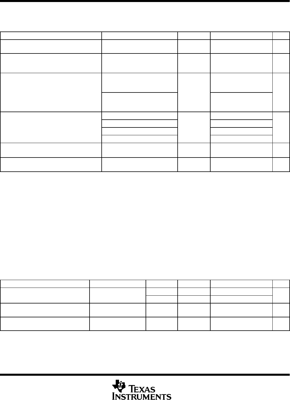
electrical characteristics over recommended ranges of supply voltage and operating free-air
temperature (unless otherwise noted) (continued)
crystal oscillator, LFXT1, low frequency modes (see Note 4)
PARAMETER TEST CONDITIONS VCC MIN TYP MAX UNIT
f
LFXT1,LF
LFXT1 oscillator crystal
frequency, LF mode 0, 1
XTS = 0, LFXT1Sx = 0 or 1 1.8 V − 3.6 V 32,768 Hz
f
LFXT1,LF,logic
LFXT1 oscillator logic level
square wave input frequency,
LF mode
XTS = 0, LFXT1Sx = 3 1.8 V − 3.6 V 10,000 32,768 50,000 Hz
Oscillation allowance for LF
XTS = 0, LFXT1Sx = 0;
f
LFXT1,LF
= 32,768 kHz,
C
L,eff
= 6 pF
500
OA
LF
crystals
XTS = 0, LFXT1Sx = 0;
f
LFXT1,LF
= 32,768 kHz,
C
L,eff
= 12 pF
200
kW
XTS = 0, XCAPx = 0 1
Integrated effective load
XTS = 0, XCAPx = 1 5.5
C
L,eff
capacitance, LF mode
see Note 1
XTS = 0, XCAPx = 2 8.5
pF
XTS = 0, XCAPx = 3 11
Duty Cycle LF mode
XTS = 0, Measured at P1.4/ACLK,
f
LFXT1,LF
= 32,768 Hz
2.2 V/3 V 30 50 70 %
f
Fault,LF
Oscillator fault frequency, LF
mode (see Note 3)
XTS = 0, LFXT1Sx = 3
(see Note 2)
2.2 V/3 V 10 10,000 Hz
NOTES: 1. Includes parasitic bond and package capacitance (approximately 2pF per pin).
Since the PCB adds additional capacitance it is recommended to verify the correct load by measuring the ACLK frequency. For a
correct setup the effective load capacitance should always match the specification of the used crystal.
2. Measured with logic level input frequency but also applies to operation with crystals.
3. Frequencies below the MIN specification set the fault flag, frequencies above the MAX specification do not set the fault flag.
Frequencies in between might set the flag.
4. To improve EMI on the LFXT1 oscillator the following guidelines should be observed.
− Keep as short a trace as possible between the device and the crystal.
− Design a good ground plane around the oscillator pins.
− Prevent crosstalk from other clock or data lines into oscillator pins XIN and XOUT.
− Avoid running PCB traces underneath or adjacent to the XIN and XOUT pins.
− Use assembly materials and praxis to avoid any parasitic load on the oscillator XIN and XOUT pins.
− If conformal coating is used, ensure that it does not induce capacitive/resistive leakage between the oscillator pins.
− Do not route the XOUT line to the JTAG header to support the serial programming adapter as shown in other
documentation. This signal is no longer required for the serial programming adapter.
internal very low power, low frequency oscillator (VLO)
PARAMETER TEST CONDITIONS T
A
VCC MIN TYP MAX UNIT
-40−85°C 2.2 V/3 V 4 12 20
f
VLO
VLO frequency
105°C 2.2 V/3 V 22
kHz
df
VLO
/dT
VLO frequency
temperature drift
(see Note 1)
I: -40−85°C
T: -40−105°C
2.2 V/3 V 0.5 %/°C
df
VLO
/dV
CC
VLO frequency supply
voltage drift
(see Note 2) 25°C 1.8V − 3.6V 4 %/V
NOTES: 1. Calculated using the box method:
I version: (MAX(−40...85_C) − MIN(−40...85_C))/MIN(−40...85_C)/(85_C − (−40_C))
T version: (MAX(−40...105_C) − MIN(−40...105_C))/MIN(−40...105_C)/(105_C − (−40_C))
2. Calculated using the box method: (MAX(1.8...3.6 V) − MIN(1.8...3.6 V))/MIN(1.8...3.6V)/(3.6 V − 1.8 V)


