Closed Dec 25th-26th
800-300-1968
We Stock Hard to Find Parts
My Account
|
My Orders
|
My Cart
Questions?
(800) 300-1968
Register
(current)
My Account
(current)
My Orders
(current)
My Cart
(current)
Categories
(current)
Manufacturers
Request a Quote
Sell Your Excess
Consignment
Quality Assurance
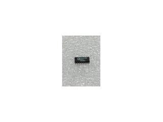
ADG408BR
Part #
ADG408BR
Description
ANLG MUX SGL 8:1 22V/32V 16SOIC N - Rail/Tube
Category
IC
Availability
Out of Stock
Qty
0
Qty
Price
1 +
$1.66577
Related Items
Analog Devices
IC
ADG406BN
$11.67902
Analog Devices
IC
ADG406BP
$24.87970
Analog Devices
IC
ADG408BN
$5.46052
Analog Devices
IC
ADG408BRU
$3.97866
Analog Devices
IC
ADG409BR
$3.95636
Fairchild Semiconductor
IC
008-25424
$11.58351