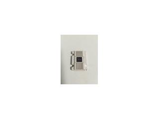
LM119QML
SNOSAN3B –JULY 2008–REVISED MARCH 2013
www.ti.com
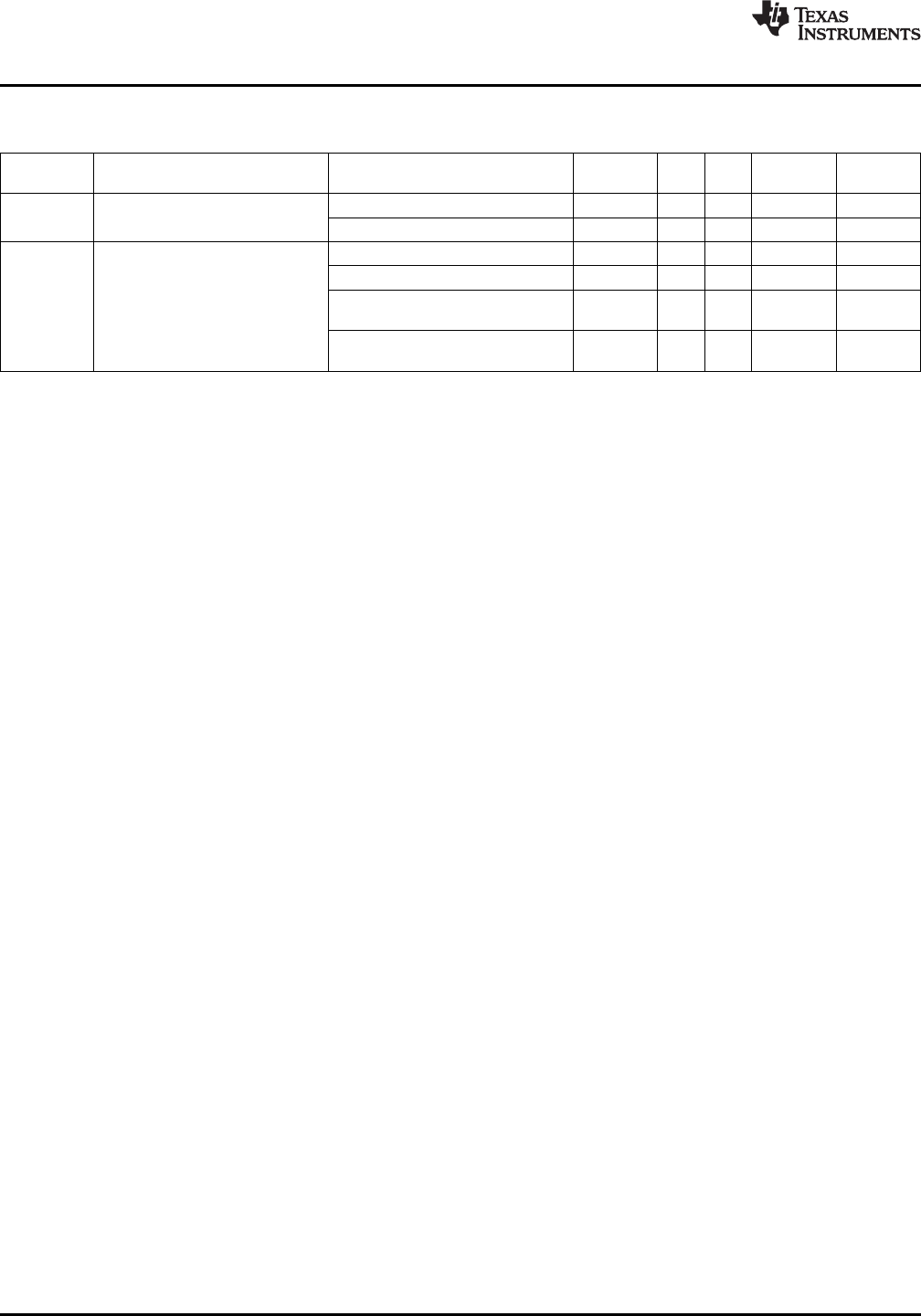
SMD 5962-9679802, ELDRS FREE 100K Post Radiation Parameters @ 25°C
(1)
The following conditions apply, unless otherwise specified. V
CM
= 0V
Sub-
Symbol Parameter Conditions Notes Min Max Units
groups
I
IB
Input Bias Current ±V
CC
= ±15V 1.0 µA 1
V
CC
= 5V 1.0 µA 1
V
IO
Input Offset Voltage
+
V
CC
= 5V, V
CM
= 1V, R
S
≤ 5KΩ -4.0 4.0 mV 1
+
V
CC
= 5V, V
CM
= 3V, R
S
≤ 5KΩ -4.0 4.0 mV 1
±V
CC
= ±15V, V
CM
= 12V, R
S
≤ -4.0 4.0 mV 1
5KΩ
±V
CC
= ±15V, V
CM
= −12V, R
S
≤ -4.0 4.0 mV 1
5KΩ
(1) Pre and post irradiation limits are identical to those listed under AC and DC electrical characteristics except as listed in the Post
Radiation Limits Table. Low dose rate testing has been performed on a wafer-by-wafer basis, per Test Method 1019, Condition D of
MIL-STD-883, with no enhanced low dose rate sensitivity (ELDRS).
10 Submit Documentation Feedback Copyright © 2008–2013, Texas Instruments Incorporated
Product Folder Links: LM119QML