Freelance Electronics Components Distributor
Closed Dec 25th-26th
800-300-1968
We Stock Hard to Find Parts

HMMC-3024

Part # HMMC-3024
Description PRESCALER 5V 1/4 12000MHZ CHIP - Gel-pak, waffle pack, waf
Category WAFER DIE
Availability In Stock
Qty 52
Qty Price
1 - 3 $77.33155
4 - 8 $61.51374
9 - 17 $57.99866
18 - 37 $53.89775
38 + $48.03930
Manufacturer Available Qty
Agilent technologies Inc
  • Shipping Freelance Stock: 50
    Ships Immediately
Agilent technologies Inc
  • Shipping Freelance Stock: 2
    Ships Immediately


Technical Document


DISCLAIMER: The information provided herein is solely for informational purposes. Customers must be aware of the suitability of this product for their application, and consider that variable factors such as Manufacturer, Product Category, Date Codes, Pictures and Descriptions may differ from available inventory.

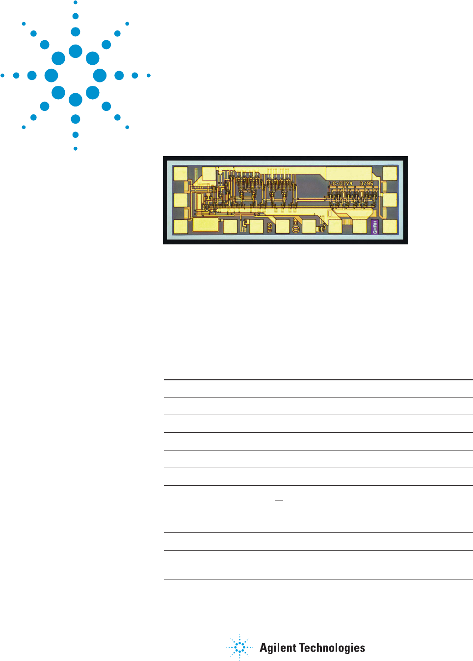
Agilent HMMC–3024
DC–12 GHz High Efficiency
GaAs HBT MMIC
Divide–by–4 Prescaler
1GC1-8007
Data Sheet
Features
Wide Frequency Range:
0.2-12 GHz
High Input Power Sensitivity:
On-chip pre- and post-amps
-25 to +10 dBm (1–8 GHz)
-15 to +18 dBm (8–10 GHz)
-10 to +2 dBm (10–12 GHz)
• Dual-mode P
out
: (Chip Form)
0 dBm (0.5 V
p–p
) @ 40 mA
-6.0 dBm (0.25 V
p–p
) @ 30 mA
• Low Phase Noise:
-153 dBc/Hz @ 100 kHz Offset
(+) or (-) Single Supply Bias
Operation
Wide Bias Supply Range:
4.5 to 6.5 volt operating range
Differential I/0 with on-chip
50 Ω matching
Description
The HMMC-3024 GaAs HBT MMIC
prescaler offers dc to 12 GHz fre-
quency translation for use in
communications and EW systems
incorporating high-frequency PLL
oscillator circuits and signal-path
down conversion applications.
The prescaler provides a large input
power sensitivity window and low
phase noise. In addition to the fea-
tures listed above the device offers
an input disable contact pad to elimi-
nate any self-oscillation condition.
Chip Size: 1330 x 440 µm (52.4 x 17.3 mils)
Chip Size Tolerance: ± 10 µm (± 0.4 mils)
Chip Thickness: 127 ± 15 µm (5.0 ± 0.6 mils)
Pad Dimensions: 70 x 70 µm (2.8 x 2.8 mils)
Absolute Maximum Ratings
1
(@ T
A
= 25°C, unless otherwise indicated)
Symbol Parameters/Conditions Min. Max. Units
V
CC
Bias supply voltage +7 volts
V
EE
Bias supply voltage -7 volts
V
CC
- V
EE
Bias supply delta 0 +7 volts
V
Disable
Pre-amp disable voltage V
EE
V
CC
volts
V
Logic
Logic threshold voltage V
CC
-1.5 V
CC
-1.2 volts
P
in(CW)
CW RF input power +10 dBm
V
RFin
DC input voltage
(@ RF
in
or RF
in
ports) V
CC
±0.5 volts
T
BS
2
Backside operating temperature -40 +85 °C
T
st
Storage temperature -65 +165 °C
T
max
Maximum assembly temperature 310 °C
(60 s max.)
Notes
1. Operation in excess of any parameter limit (except T
BS
) may cause permanent damage to the device.
2. MTTF > 1 x 10
6
hours @ T
BS
85°C. Operation in excess of maximum operating temperature (T
BS
) will degrade MTTF.
2
Symbol Parameters/Conditions Min. Typ. Max. Units
V
CC
– V
EE
Operating bias supply difference
1
4.5 5.0 6.5 volts
|I
CC
| or |I
EE
| Bias supply current
(HIGH Output Power Confi guration
2
: V
PwrSel
= V
EE
) 34 40 46 mA
Bias supply current
(LOW Output Power Confi guration: V
PwrSel
= open) 25 30 35 mA
V
RFin(q)
Quiescent dc voltage appearing at all RF ports V
CC
volts
V
RFout(q)
V
Logic
Nominal ECL Logic Level
(V
Logic
contact self-bias voltage, generated on-chip) V
CC
-1.45 V
CC
-1.32 V
CC
-1.25 volts
Notes
1. Prescaler will operate over full specifi ed supply voltage range, V
CC
or V
EE
not to exceed limits specifi ed in Absolute Maximum Ratings section.
2. High output power confi guration: P
out
= 0 dBm (V
out
= 0.5 V
p-p
). Low output power confi guration: P
out
= -6.0 dBm (V
out
= 0.25 V
p-p
)
dc Specifi cations/Physical Properties
(T
A
= 25°C, V
CC
– V
EE
= 5.0 volts, unless otherwise listed)
Symbol Parameters/Conditions Min. Typ. Max. Units
ƒ
in(max)
Maximum input frequency of operation 12 14 GHz
ƒ
in(min)
Minimum input frequency of operation
1
0.2 0.5 GHz
(P
in
= -10 dBm)
ƒ
Self–Osc.
Output Self-Oscillation Frequency
2
3.4 GHz
P
in
@ dc, (Square-wave input) -15 > -25 +10 dBm
@ ƒ
in
= 500 MHz, (Sine-wave input) -15 > -20 +10 dBm
ƒ
in
= 1 to 8 GHz -15 > -20 +10 dBm
ƒ
in
= 8 to 10 GHz -10 > -15 + 5 dBm
ƒ
in
= 10 to 12 GHz -5 > -10 -1 dBm
RL Small-Signal Input/Output Return Loss (@ ƒ
in
< 10 GHz) 15 dB
S
12
Small-Signal Reverse Isolation (@ ƒ
in
< 10 GHz) 30 dB
φ
N
SSB Phase noise (@ P
in
= 0 dBm, 100 kHz offset from a -153 dBc/Hz
ƒ
out
= 1.2 GHz Carrier)
Jitter Input signal time variation @ zero–crossing 1 ps
in
= 10 GHz, P
in
= -10 dBm)
T
r
or T
f
Output edge speed (10% to 90% rise/fall time) 70 ps
Notes
1. For sine-wave input signal. Prescaler will operate down to D.C. for square-wave input signal. Minimum divide frequency limited by input slew-rate.
2. Prescaler may exhibit this output signal under bias in the absence of an RF input signal. This condition may be eliminated by use of the Pre-amp
Disable ( V
Disable
) feature, or the Differential Input de-biasing technique.
RF Specifi cations
(T
A
= 25°C, Z
0
= 50 , V
CC
– V
EE
= 5.0 volts) (÷4)
3
High Output Power Operating Mode
1
Symbol Parameters/Conditions Min. Typ. Max. Units
P
out
@ ƒ
out
< 1 GHz -2.0 0.0 dBM
@ ƒ
out
= 2.5 GHz -2.5 -0.5 dBm
@ ƒ
out
= 3.0 GHz -3.0 -1.0 dBm
|V
out(p–p)
| @ ƒ
out
< 1 GHz 0.39 0.5 volts
@ ƒ
out
= 2.5 GHz 0.37 0.47 volts
@ ƒ
out
= 3.0 GHz 0.35 0.44 volts
P
Spitback
ƒ
out
power level appearing at RF
in
or RF
in
-53 dBm
(@ ƒ
in
10 GHz, Unused RF
out
or RF
out
unterminated)
ƒ
out
power level appearing at RF
in
or RF
in
-73 dBm
(@ ƒ
in
= 10 GHz, Both RF
out
& RF
out
terminated)
P
feedthru
Power level of ƒ
in
appearing at RF
out
or RF
out
-30 dBc
(@ ƒ
in
= 12 GHz, P
in
= 0 dBm, referred to P
in
in
)
H
2
Second harmonic distortion output level
(@ ƒ
out
= 3.0 GHz, referred to P
out
out
)) -25 dBc
Low Output Power Operating Mode
2
P
out
@ ƒ
out
< 1 GHz -8.0 -6.0 dBm
@ ƒ
out
= 2.5 GHz -8.5 -6.5 dBm
@ ƒ
out
= 3.0 GHz -9.0 -7.0 dBm
|V
out(p–p)
| @ ƒ
out
< 1 GHz 0.20 0.25 volts
@ ƒ
out
= 2.5 GHz 0.19 0.24 volts
@ ƒ
out
= 3.0 GHz 0.18 0.22 volts
P
Spitback
ƒ
out
power level appearing at RF
in
or RF
in
(@ ƒ
in
12 GHz, Unused RF
out
or RF
out
unterminated) -61 dBm
ƒ
out
power level appearing at RF
in
or RF
in
(@ ƒ
in
= 12 GHz, both RF
out
& RF
out
terminated) -82 dBm
P
feedthru
Power level of ƒ
in
appearing at RF
out
or RF
out
(@ ƒ
in
= 12 GHz, P
in
= 0 dBm, referred to P
in
in
)) -30 dBc
H
2
Second harmonic distortion output level
(@ ƒ
out
= 3.0 GHz, referred to P
out
out
)) -30 dBc
Notes
1. V
PwrSel
= V
EE
.
2. V
PwrSel
= Open Circuit.
RF Specifi cations (Continued)
(T
A
= 25°C, Z
0
= 50 , V
CC
– V
EE
= 5.0 volts)
123NEXT