Closed Dec 25th-26th
800-300-1968
We Stock Hard to Find Parts
My Account
|
My Orders
|
My Cart
Questions?
(800) 300-1968
Register
(current)
My Account
(current)
My Orders
(current)
My Cart
(current)
Categories
(current)
Manufacturers
Request a Quote
Sell Your Excess
Consignment
Quality Assurance
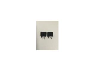
IRF640NS
Part #
IRF640NS
Description
Trans MOSFET N-CH 200V 18A 3-Pin(2+Tab) D2PAK
Category
TRANSISTOR
Availability
Out of Stock
Qty
0
Qty
Price
1 +
$2.58112
Related Items
International Rectifier
VOLTAGE REGULAT
IRF640
$4.44227
International Rectifier
RECTIFIER
IRF640N
$1.44163
International Rectifier
RECTIFIER
IRF640S
$0.24552
International Rectifier
RECTIFIER
IRF640SI
Solitron
TRANSISTOR
001021
$15.91144
Military Spec
TRANSISTOR
0012B