Closed Dec 25th-26th
800-300-1968
We Stock Hard to Find Parts
My Account
|
My Orders
|
My Cart
Questions?
(800) 300-1968
Register
(current)
My Account
(current)
My Orders
(current)
My Cart
(current)
Categories
(current)
Manufacturers
Request a Quote
Sell Your Excess
Consignment
Quality Assurance
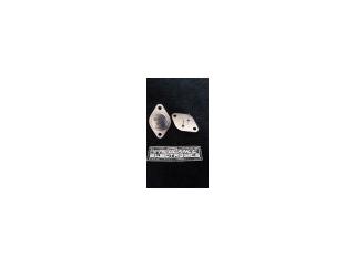
IRF3205
Part #
IRF3205
Description
Trans MOSFET N-CH 55V 110A 3-Pin(3+Tab) TO-220AB - Rail/Tu
Category
TRANSISTOR
Availability
Out of Stock
Qty
0
Qty
Price
1 +
$1.81918
Related Items
SAMSUNG ELECTRONICS
TRANSISTOR
IRF320
$2.02728
International Rectifier
TRANSISTOR
IRF3205S
$1.52965
International Rectifier
RECTIFIER
IRF3205SRB
$12.83939
Solitron
TRANSISTOR
001021
$15.91144
Military Spec
TRANSISTOR
0012B
Military Spec
TRANSISTOR
01001
$59.68129