Closed Dec 25th-26th
800-300-1968
We Stock Hard to Find Parts
My Account
|
My Orders
|
My Cart
Questions?
(800) 300-1968
Register
(current)
My Account
(current)
My Orders
(current)
My Cart
(current)
Categories
(current)
Manufacturers
Request a Quote
Sell Your Excess
Consignment
Quality Assurance
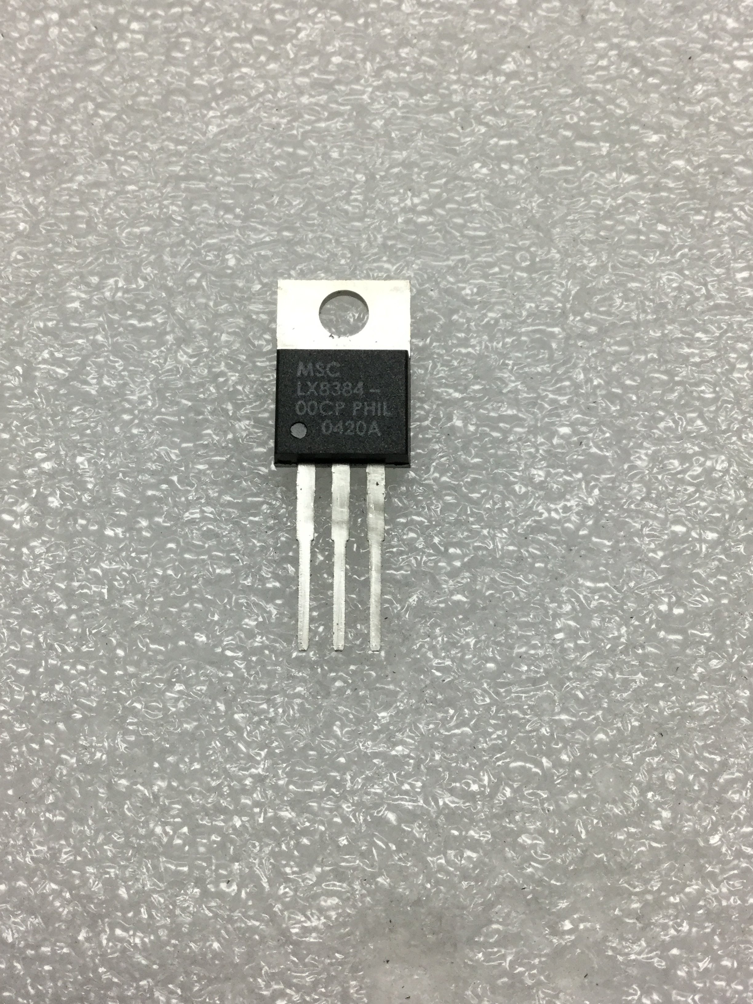
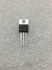
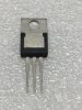
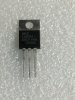
LX8384-00CP
Part #
LX8384-00CP
Description
IC REG LDO ADJ 5A TO220
Category
RECTIFIER
Availability
In Stock
Qty
217
Qty
Price
1 - 45
$5.25559
46 - 91
$4.18059
92 - 136
$3.94169
137 - 182
$3.66299
183 +
$3.26484
Manufacturer
Available
Qty
Linfinity Microelectronics Inc
Date Code: 9634
Freelance Stock:
153
Ships Immediately
Microsemi Corp
Date Code: 0420
Freelance Stock:
64
Ships Immediately
Add to Cart
Related Items
Linfinity Microelectronics Inc
RECTIFIER
LX8382A-33CV
$7.88804
Linfinity Microelectronics Inc
RECTIFIER
LX8385-00CDD
$6.33661
International Rectifier
RECTIFIER
10BQ060
$0.28930
International Rectifier
RECTIFIER
10CTQ150S
$2.10035
International Rectifier
RECTIFIER
10MQ060NTRPBF
$0.42140
International Rectifier
RECTIFIER
10TQ045
$0.75375