Closed Dec 25th-26th
800-300-1968
We Stock Hard to Find Parts
My Account
|
My Orders
|
My Cart
Questions?
(800) 300-1968
Register
(current)
My Account
(current)
My Orders
(current)
My Cart
(current)
Categories
(current)
Manufacturers
Request a Quote
Sell Your Excess
Consignment
Quality Assurance
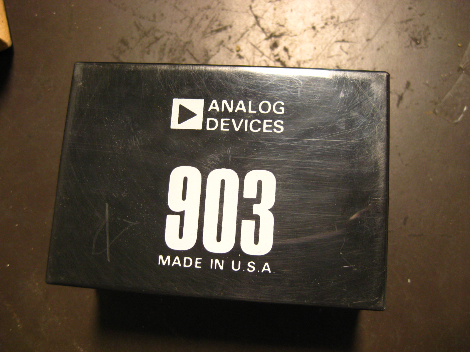
903
Part #
903
Description
Power Supply Module 4PinPlastic
Category
POWER SUPPLY
Availability
In Stock
Qty
1
Qty
Price
1 +
$104.44467
Manufacturer
Available
Qty
Analog Devices
Date Code: 8312
Freelance Stock:
1
Ships Immediately
Add to Cart
Related Items
Analog Devices
POWER SUPPLY
903
$104.44467
Hughes Aircraft Company
POWER SUPPLY
001378
POWERSPEC
POWER SUPPLY
02-00227-02
2D627
POWER SUPPLY
02005-60149-102
Generic
POWER SUPPLY
021-425-22
Generic
POWER SUPPLY
033-61001612