6-66
HMMC-5618 Applications
The HMMC-5618 is a GaAs MMIC
amplifier designed for optimum
Class-A efficiency and flat gain
performance from 6 GHz to
20␣ GHz. It has applications as a
cascadable gain stage for EW
amplifiers, buffer stages, LO
drives, phased-array radar, and
transmitter amplifiers used in
commercial communication
systems. The MMIC solution is a
cost effective alternative to
hybrid assemblies.
Biasing and Operation
The MMIC amplifier is normally
biased with a single positive drain
supply connected to both V
D1
and
V
D2
bond pads as shown in
Figure␣ 8a. The recommended
drain supply voltage is 3 to
5␣ volts. If desired, the first stage
drain bonding pad can be biased
separately to provide a small
amount of gain slope control or
bandwidth extension as demon-
strated in Figure 2.
No ground wires are required
because all ground connections
are made with plated through-
holes to the backside of the
device.
Gate bias pads (V
G1
and V
G2
) are
also provided to allow adjust-
ments in gain, RF output power,
and DC power dissipation, if
necessary. No connection to the
gate pads is needed for single
drain-bias operation. However,
for custom applications, the DC
current flowing through the input
and/or output gain stage may be
adjusted by applying a voltage to
the gate bias pad(s) as shown in
Figure 8b. A negative gate-pad
voltage will decrease the drain
current. The gate-pad voltage is
approximately zero volts during
operation with no DC gate supply.
Refer to the Absolute Maximum
Ratings table for allowed DC and
thermal conditions.
Assembly Techniques
Solder die attach using a fluxless
gold-tin (AuSn) solder preform is
the recommended assembly
method. A conductive epoxy such
as ABLEBOND
®
71-1LM1 or
ABLEBOND
®
36-2 may also be
used for die attaching provided
the Maximum Thermal Ratings
are not exceeded. The device
should be attached to an electri-
cally conductive surface to
complete the DC and RF ground
paths. The backside metallization
on the device is gold.
It is recommended that the RF
input, RF output, and DC supply
connections be made using
0.7␣ mil diameter gold wire. The
device has been designed so that
optimum performance is realized
when the RF input and RF output
bond-wire inductance is approxi-
mately 0.2␣ nH as demonstrated in
Figures 4, 6, and 7. Therefore,
mesh or multiple-wire bonds are
not necessary. It is, however,
recommended that the RF wires
be as short as possible to mini-
mize assembly related perfor-
mance variations.
Thermosonic wedge is the
preferred method for wire
bonding to the gold bond pads.
Wires can be attached using a
guided-wedge at an ultrasonic
power level of roughly 64 dB for a
duration of 76 ± 8 msec with a
stage temperature of 150 ± 2 °C.
For more detailed information
see HP application note #999
“GaAs MMIC Assembly and
Handling Guidelines.”
GaAs MMICs are ESD sensitive.
Proper precautions should be used
when handling these devices.
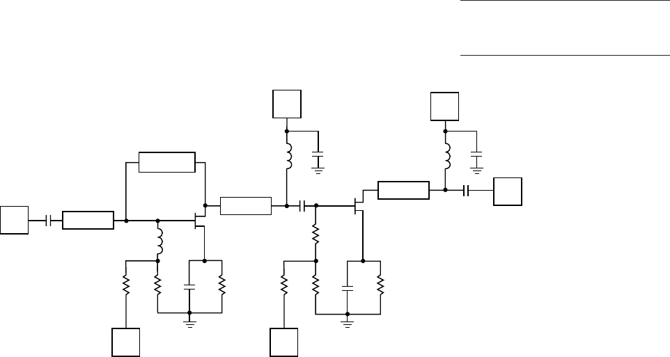
Figure 1. HMMC-5618 Simplified Schematic.
IN
V
G1
V
G2
2KΩ 2KΩ 2KΩ 1KΩ
OUT
MATCHING
MATCHING
FEEDBACK
NETWORK
MATCHING
V
D1
V
D2


