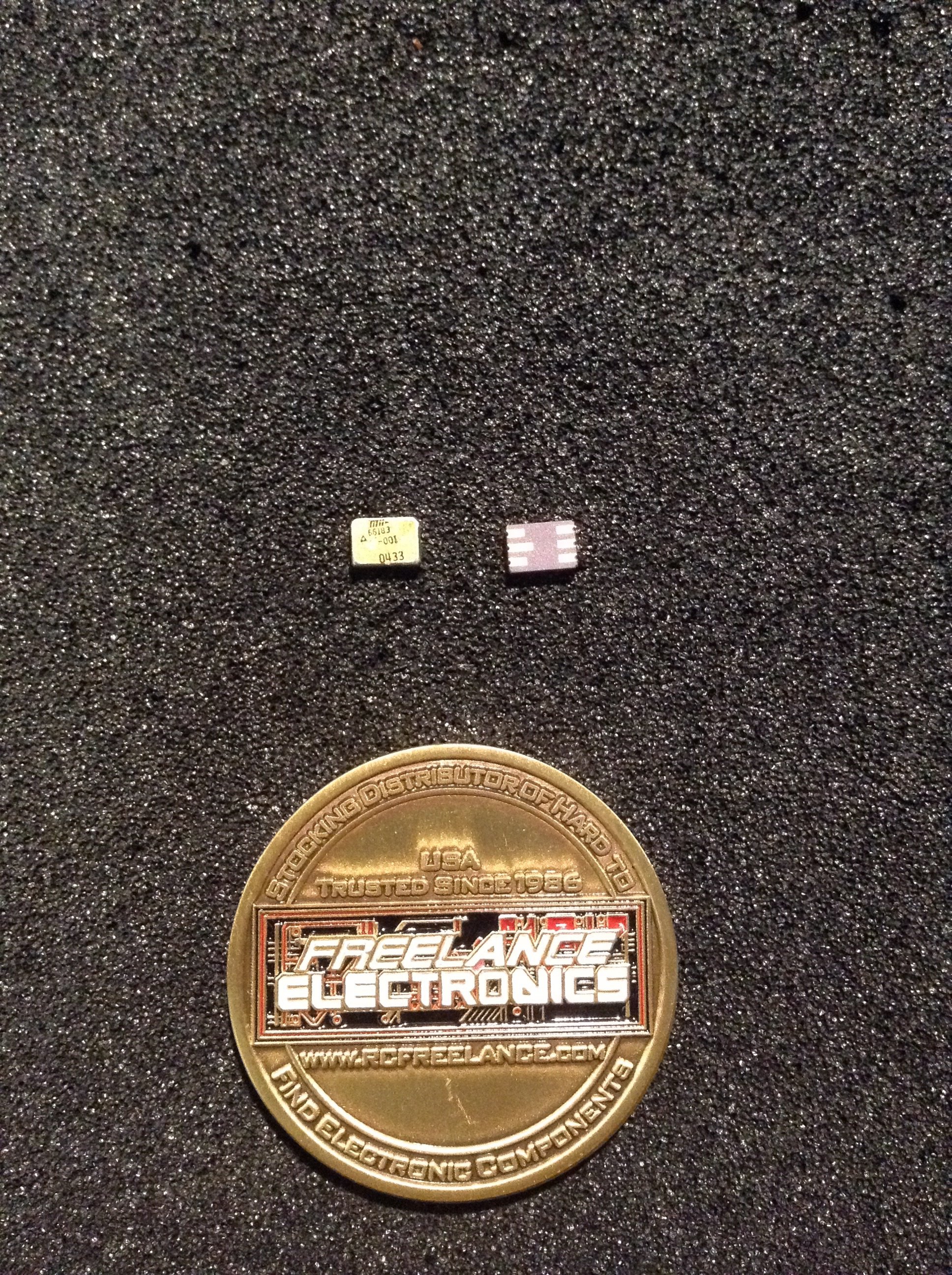
Freelance Electronics Components Distributor
Closed Dec 25th-26th
800-300-1968
We Stock Hard to Find Parts

66183-001

Part # 66183-001
Description Optocoupler DC-IN 1-CH Transistor W/ Base DC-OUT 6-LCC
Category Microcircuit
Availability In Stock
Qty 33
Qty Price
1 - 1 $173.39438
2 - 3 $137.92735
4 - 7 $130.04579
8 - 16 $120.85063
17 + $107.71469
Manufacturer Available Qty
MICRO PAC
Date Code: 0433
  • Shipping Freelance Stock: 15
    Ships Immediately
MICRO PAC
Date Code: 0433
  • Shipping Freelance Stock: 18
    Ships Immediately


Technical Document


DISCLAIMER: The information provided herein is solely for informational purposes. Customers must be aware of the suitability of this product for their application, and consider that variable factors such as Manufacturer, Product Category, Date Codes, Pictures and Descriptions may differ from available inventory.

MICROPAC INDUSTRIES, INC.
OPTOELECTRONIC PRODUCTS DIVISION
725 E.Walnut Str., Garland, TX 75040
(972)272-3571
Fax (972)487-6918
www.micropac.com
E-MAIL: OPTOSALES @ MICROPAC.COM
5 - 40
66183
PROTON RADIATION TOLERANT OPTOCOUPLER
(Single Channel, Electrically Similar to 4N49)
Mii
OPTOELECTRONIC PRODUCTS
DIVISION
REVISION C 5/6/02
Features:
High Reliability
Base lead provided for conventional transistor
biasing
Rugged package
Stability over wide temperature
+1000V electrical isolation
Applications:
Eliminate ground loops
Level shifting
Line receiver
Switching power supplies
Motor control
DESCRIPTION
The
66183
is a single channel device electrically similar to the 4N49. This product has been designed to be more tolerant to
proton radiation. The 66183 optocoupler is packaged in a hermetically sealed 6 pin leadless chip carrier (LCC). This device
can be supplied to customer specifications as well as tested in accordance with MIL-PRF-19500 to Class S level.
ABSOLUTE MAXIMUM RATINGS
Input to Output Voltage........................................................................................................................................................... 1kV
Emitter-Base Voltage................................................................................................................................................................7V
Collector-Emitter Voltage (Value applies to emitter-base open-circuited & the input-diode equal to zero) ......................... 40V
Collector-Base Voltage ...........................................................................................................................................................45V
Reverse Input Voltage ............................................................................................................................................................. 2V
Input Diode Continuous Forward Current at (or below) 65°C Free-Air Temperature (see note 1) ................................... 50mA
Peak Forward Input Current (Value applies for tw
1
µ
s, PRR
<
300 pps) ............................................................................. 1A
Continuous Collector Current ..............................................................................................................................................50mA
Continuous Transistor Power Dissipation at (or below) 25
°
C Free-Air Temperature (see Note 2)................................ 300mW
Storage Temperature......................................................................................................................................... -55°C to +150°C
Operating Free-Air Temperature Range ............................................................................................................-55°C to +100°C
Lead Solder Temperature (10 seconds max.) .................................................................................................................. 240°C
Notes:
1. Derate linearly to 100°C free-air temperature at the rate of 0.80 mW/°C above 25°C.
2. Derate linearly to 100°C free-air temperature at the rate of 3 mW/°C above 25
°
C.
Package Dimensions Schematic Diagram
PIN 1
IDENTIFIER
2
1
6
5
4
3
ALL DIMENSIONS ARE IN INCHES [MILLIMETERS]
0.253 [6.42]
0.237 [6.01]
0.087 [2.22]
0.071 [1.81]
0.036 [0.91]
0.020 [0.51]
0.113 [2.87]
0.097 [2.46]
0.098 [2.49]
0.082 [2.08]
0.078 [1.99]
0.062 [1.58]
0.045 [1.14]
0.055 [1.40]
0.178 [4.52]
0.162 [4.11]
1
6
3
5
4
B
E
C
MICROPAC INDUSTRIES, INC.
OPTOELECTRONIC PRODUCTS DIVISION
725 E.Walnut Str., Garland, TX 75040
(972)272-3571
Fax (972)487-6918
www.micropac.com
E-MAIL: OPTOSALES @ MICROPAC.COM
5 - 41
66183
PROTON RADIATION TOLERANT OPTOCOUPLER
(Electrically similar to 4N49)
REVISION C 5/6/02
ELECTRICAL CHARACTERISTICS
T
A
= 25
°
C unless otherwise specified.
PARAMETER SYMBOL MIN TYP MAX UNITS TEST CONDITIONS NOTE
Input Diode Static Reverse Current I
R
100 µA V
R
= 3V
Input Diode Static Forward Voltage -55
°
C V
F
1.0 2.2 V I
F
= 10mA
Input Diode Static Forward Voltage +25
°
C V
F
0.8 1.8 2.0 V I
F
= 10mA
Input Diode Static Forward Voltage +100
°
C V
F
0.8 2.2 V I
F
= 10mA
OUTPUT TRANSISTOR
T
A
= 25
°
C unless otherwise specified.
PARAMETER SYMBOL MIN TYP MAX UNITS TEST CONDITIONS NOTE
Collector-Base Breakdown Voltage V
(BR)CBO
45 V I
C
= 100
µ
A, I
B
= 0, I
F
= 0
Collector-Emitter Breakdown Voltage V
(BR)CEO
40 V I
C
= 1mA, I
B
= 0, I
F
= 0
Emitter-Base Breakdown Voltage V
(BR)EBO
2
V I
C
= 0mA, I
E
= 100
µ
A, I
F
= 0
Off-State Collector Current
+100
°
C
I
CEO
I
CEO
100
100
nA
µ
A
V
CE
= 20V, I
F
= 0mA, I
B
= 0
V
CE
= 20V, I
F
= 0mA, I
B
= 0
COUPLED CHARACTERISTICS
T
A
= 25
°
C unless otherwise specified.
PARAMETER SYMBOL MIN TYP MAX UNITS TEST CONDITIONS NOTE
On State Collector Current I
C(ON)
2.0 mA V
CE
= 5V, I
F
= 1mA, I
B
=0
On State Collector Current +100
°
C I
C(ON)
2.0 mA V
CE
= 5.0V, I
F
= 2mA, I
B
=0
On State Collector Current -55
°
C I
C(ON)
2.8 mA V
CE
= 5V, I
F
= 2mA, I
B
=0
Collector-Emitter Saturation Voltage V
CE(SAT)
0.3 V I
F
= 2mA, I
C
= 2mA
Input to Output Internal Resistance R
IO
10
11
V
IN-OUT
= 1000V
1
Input to Output Capacitance C
IO
2.5 5 pF f = 1MHz, V
IN-OUT
= 1000V 1
Rise Time-Phototransistor Operation
t
r
10 25
µ
s V
CC
= 10V, I
F
= 10mA,
R
L
= 100
, I
B
= 0
Fall Time-Phototransistor Operation
t
f
10 25
µ
s V
CC
= 10V, I
F
= 10mA,
R
L
= 100
, I
B
= 0
NOTES:
1. These parameters are measured between all phototransistor leads shorted together and with both input diode leads shorted together.
2. This parameter must be measured using pulse techniques (t
W
= 100
µ
s duty cycle
<
1%).
RECOMMENDED OPERATING CONDITIONS:
PARAMETER SYMBOL MIN MAX UNITS
Input Current, Low Level I
FL
0 90
µ
A
Input Current, High Level I
FH
2 10 mA
Supply Voltage V
CE
5 10 V
Operating Temperature T
A
-55 100
°
C
SELECTION GUIDE
PART NUMBER PART DESCRIPTION
66183-001 Single channel proton radiation tolerant optocoupler - commercial
66183-101 Single channel proton radiation tolerant optocoupler – screened to JAN
66183-103 Single channel proton radiation tolerant optocoupler – screened to JANTX
66183-105 Single channel proton radiation tolerant optocoupler – screened to JANTXV