Freelance Electronics Components Distributor
Closed Dec 25th-26th
800-300-1968
We Stock Hard to Find Parts

SN74LVT16501DGGR

Part # SN74LVT16501DGGR
Description Bus XCVR Single 18-CH 3-ST 56-Pin TSSOP T/R - Tape and Ree
Category IC
Availability In Stock
Qty 40
Qty Price
1 - 8 $1.02296
9 - 16 $0.81372
17 - 25 $0.76722
26 - 33 $0.71297
34 + $0.63548
Manufacturer Available Qty
Texas Instruments
  • Shipping Freelance Stock: 40
    Ships Immediately


Technical Document


DISCLAIMER: The information provided herein is solely for informational purposes. Customers must be aware of the suitability of this product for their application, and consider that variable factors such as Manufacturer, Product Category, Date Codes, Pictures and Descriptions may differ from available inventory.

SN54LVT16501, SN74LVT16501
3.3-V ABT 18-BIT UNIVERSAL BUS TRANSCEIVERS
WITH 3-STATE OUTPUTS
SCBS147G – MAY 1992 – REVISED NOVEMBER 1996
1
POST OFFICE BOX 655303 DALLAS, TEXAS 75265
State-of-the-Art Advanced BiCMOS
Technology (ABT) Design for 3.3-V
Operation and Low-Static Power
Dissipation
Members of the Texas Instruments
Widebus
Family
Support Mixed-Mode Signal Operation (5-V
Input and Output Voltages With 3.3-V V
CC
)
Support Unregulated Battery Operation
Down to 2.7 V
UBT
(Universal Bus Transceiver)
Combines D-Type Latches and D-Type
Flip-Flops for Operation in Transparent,
Latched, or Clocked Mode
Typical V
OLP
(Output Ground Bounce)
< 0.8 V at V
CC
= 3.3 V, T
A
= 25°C
ESD Protection Exceeds 2000 V Per
MIL-STD-883, Method 3015; Exceeds 200 V
Using Machine Model
(C = 200 pF, R = 0)
Latch-Up Performance Exceeds 500 mA
Per JEDEC Standard JESD-17
Bus Hold on Data Inputs Eliminates the
Need for External Pullup/Pulldown
Resistors
Support Live Insertion
Distributed V
CC
and GND Pin Configuration
Minimizes High-Speed Switching Noise
Flow-Through Architecture Optimizes
PCB Layout
Package Options Include Plastic 300-mil
Shrink Small-Outline (DL) and Thin Shrink
Small-Outline (DGG) Packages and 380-mil
Fine-Pitch Ceramic Flat (WD) Package
Using 25-mil Center-to-Center Spacings
description
The ’LVT16501 are 18-bit universal bus transceivers designed for low-voltage (3.3-V) V
CC
operation, but with
the capability to provide a TTL interface to a 5-V system environment.
Data flow in each direction is controlled by output-enable (OEAB and OEBA), latch-enable (LEAB and LEBA),
and clock (CLKAB and CLKBA) inputs. For A-to-B data flow, the devices operate in the transparent mode when
LEAB is high. When LEAB is low, the A data is latched if CLKAB is held at a high or low logic level. If LEAB is
low, the A-bus data is stored in the latch/flip-flop on the low-to-high transition of CLKAB. When OEAB is high,
the outputs are active. When OEAB is low, the outputs are in the high-impedance state.
Copyright 1996, Texas Instruments Incorporated
PRODUCTION DATA information is current as of publication date.
Products conform to specifications per the terms of Texas Instruments
standard warranty. Production processing does not necessarily include
testing of all parameters.
Please be aware that an important notice concerning availability, standard warranty, and use in critical applications of
Texas Instruments semiconductor products and disclaimers thereto appears at the end of this data sheet.
Widebus and UBT are trademarks of Texas Instruments Incorporated.
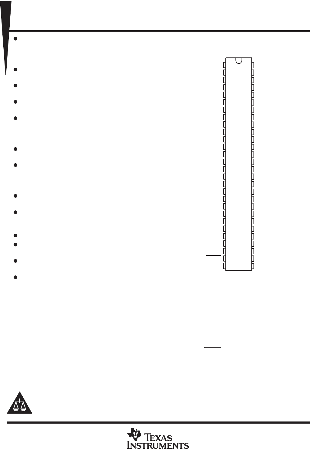
SN54LVT16501 . . . WD PACKAGE
SN74LVT16501 . . . DGG OR DL PACKAGE
(TOP VIEW)
1
2
3
4
5
6
7
8
9
10
11
12
13
14
15
16
17
18
19
20
21
22
23
24
25
26
27
28
56
55
54
53
52
51
50
49
48
47
46
45
44
43
42
41
40
39
38
37
36
35
34
33
32
31
30
29
OEAB
LEAB
A1
GND
A2
A3
V
CC
A4
A5
A6
GND
A7
A8
A9
A10
A11
A12
GND
A13
A14
A15
V
CC
A16
A17
GND
A18
OEBA
LEBA
GND
CLKAB
B1
GND
B2
B3
V
CC
B4
B5
B6
GND
B7
B8
B9
B10
B11
B12
GND
B13
B14
B15
V
CC
B16
B17
GND
B18
CLKBA
GND
SN54LVT16501, SN74LVT16501
3.3-V ABT 18-BIT UNIVERSAL BUS TRANSCEIVERS
WITH 3-STATE OUTPUTS
SCBS147G – MAY 1992 – REVISED NOVEMBER 1996
2
POST OFFICE BOX 655303 DALLAS, TEXAS 75265
description (continued)
Data flow for B to A is similar to that of A to B but uses OEBA, LEBA, and CLKBA. The output enables are
complementary (OEAB is active high and OEBA is active low).
Active bus-hold circuitry is provided to hold unused or floating data inputs at a valid logic level.
To ensure the high-impedance state during power up or power down, OE should be tied to V
CC
through a pullup
resistor. The minimum value of the resistor is determined by the current-sinking capability of the driver. OE
should be tied to GND through a pulldown resistor; the minimum value of the resistor is determined by the
current-sourcing capability of the driver.
The SN74LVT16501 is available in TI’s shrink small-outline (DL) and thin shrink small-outline (DGG) packages,
which provide twice the input/output (I/O) pin count and functionality of standard small-outline packages in the
same printed circuit board area.
The SN54LVT16501 is characterized for operation over the full military temperature range of –55°C to 125°C.
The SN74LVT16501 is characterized for operation from –40°C to 85°C.
FUNCTION TABLE
INPUTS
OUTPUT
OEAB LEAB CLKAB A
B
L X X X Z
H HXLL
H HXHH
H L LL
H L HH
H LHXB
0
H L L X B
0
§
A-to-B data flow is shown; B-to-A flow is similar but
uses OEBA
, LEBA, and CLKBA.
Output level before the indicated steady-state input
conditions were established, provided that CLKAB
was high before LEAB went low
§
Output level before the indicated steady-state input
conditions were established
SN54LVT16501, SN74LVT16501
3.3-V ABT 18-BIT UNIVERSAL BUS TRANSCEIVERS
WITH 3-STATE OUTPUTS
SCBS147G – MAY 1992 – REVISED NOVEMBER 1996
3
POST OFFICE BOX 655303 DALLAS, TEXAS 75265
logic symbol
A2
5
EN1
1
OEAB
2C3
3D
3
A1 B1
54
A14
20
A15
21
A16
23
A17
24
A8
13
A9
14
A10
15
A11
16
A12
17
A3
6
A4
8
A5
9
A6
10
A7
12
B13
38
B14
37
B15
36
B16
34
B17
33
B18
31
6D
4
A18
26
B8
44
B9
43
B10
42
B11
41
B12
40
B3
51
B4
49
B5
48
B6
47
B7
45
B2
52
C6
28
LEBA
G5
30
CLKBA
EN4
27
C3
2
LEAB
G2
55
CLKAB
5C6
OEBA
11
1
A13
19
This symbol is in accordance with ANSI/IEEE Std 91-1984 and IEC Publication 617-12.
1234NEXT