Closed Dec 25th-26th
800-300-1968
We Stock Hard to Find Parts
My Account
|
My Orders
|
My Cart
Questions?
(800) 300-1968
Register
(current)
My Account
(current)
My Orders
(current)
My Cart
(current)
Categories
(current)
Manufacturers
Request a Quote
Sell Your Excess
Consignment
Quality Assurance
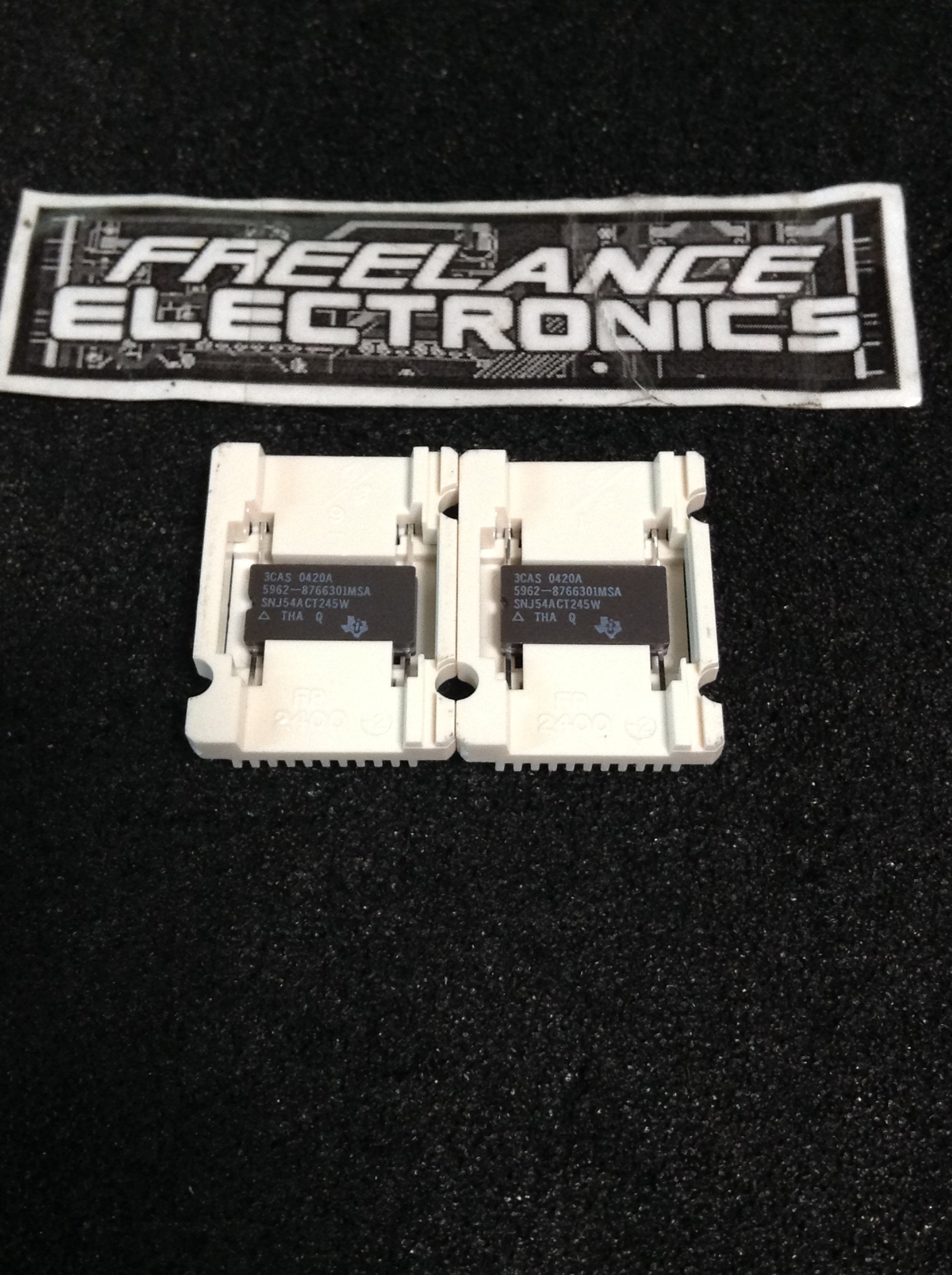
SNJ54ACT245W
Part #
SNJ54ACT245W
Description
Bus XCVR Single 8-CH 3-ST 20-Pin CFPAK Tube - Rail/Tube (A
Category
IC
Availability
In Stock
Qty
4
Qty
Price
1 - 2
$21.27230
3 +
$16.11538
Manufacturer
Available
Qty
Texas Instruments
Date Code: 0420
Freelance Stock:
4
Ships Immediately
Add to Cart
Related Items
Texas Instruments
IC
SNJ5400W
$12.21486
Texas Instruments
IC
SNJ5401J
$8.42824
Texas Instruments
IC
SNJ5401W
$11.13799
Texas Instruments
IC
SNJ5402J
$3.21444
Texas Instruments
IC
SNJ5405J
$7.95957
Texas Instruments
IC
SNJ5405W
$11.25051