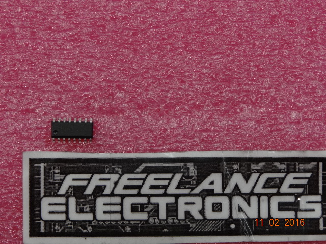
Freelance Electronics Components Distributor
Closed Dec 25th-26th
800-300-1968
We Stock Hard to Find Parts

MAX312FESE

Part # MAX312FESE
Description Analog Switch Quad SPST 16-Pin SOIC N - Rail/Tube (Alt: MA
Category IC
Availability In Stock
Qty 29
Qty Price
1 - 6 $17.37631
7 - 12 $13.82206
13 - 18 $13.03223
19 - 24 $12.11076
25 + $10.79437
Manufacturer Available Qty
MAXIM
Date Code: 0248
  • Shipping Freelance Stock: 21
    Ships Immediately
MAXIM
Date Code: 0248
  • Shipping Freelance Stock: 6
    Ships Immediately
MAXIM
Date Code: 0346
  • Shipping Freelance Stock: 2
    Ships Immediately


Technical Document


DISCLAIMER: The information provided herein is solely for informational purposes. Customers must be aware of the suitability of this product for their application, and consider that variable factors such as Manufacturer, Product Category, Date Codes, Pictures and Descriptions may differ from available inventory.

General Description
The MAX312F/MAX313F/MAX314F are quad, single-
pole/single-throw (SPST), fault-protected analog switch-
es. They are pin compatible with the industry-standard
nonprotected MAX312/MAX313/MAX314. These switch-
es feature fault-protected inputs and Rail-to-Rail
signal-
handling capability. All analog signal terminals are pro-
tected from overvoltage faults up to ±36V with power on
and up to ±40V with power off. During a fault condition,
the COM_, NO_, or NC_ terminal becomes an open cir-
cuit and only microamperes of leakage current flow from
the source. On-resistance is 10 (max) and is matched
between switches to 0.5 (max) at +25°C.
The MAX312F has four normally closed (NC) switches.
The MAX313F has four normally open (NO) switches.
The MAX314F has two NC and two NO switches. These
CMOS switches operate with dual power supplies rang-
ing from ±4.5V to ±20V or a single supply between +9V
and +36V. All digital inputs have +0.8V and +2.4V logic
thresholds, ensuring both TTL and CMOS logic com-
patibility when using ±15V or a single +12V supply.
For supply voltages of ±5V, +5V, and +3V, refer to the
MAX4711/MAX4712/MAX4713 data sheet.
Applications
Communications Systems
Signal Routing
Test Equipment
Data Acquisition
Industrial and Process Control Systems
Avionics
Redundant/Backup Systems
ATE
Hot Swap
Features
No Power-Supply Sequencing Required
Rail-to-Rail Signal Handling
All Switches Off with Power Off
All Switches Off when V+ is Off and V- is On
±40V Fault Protection with Power Off
±36V Fault Protection with ±15V Supplies
Control Line Fault Protection from
V- - 0.3V to V- + 40V
Pin Compatible with Industry-Standard
DG411/DG412/DG413
600ns (typ) Fault Response Time
10 (max) R
ON
with ±15V Supplies
±4.5V to ±20V Dual Supplies
+9V to +36V Single Supply
TTL- and CMOS-Compatible Logic Inputs with
±15V or Single +9V to +15V Supplies
MAX312F/MAX313F/MAX314F
Quad, Rail-to-Rail, Fault-Protected,
SPST Analog Switches
19-2737; Rev 0; 1/03
For pricing, delivery, and ordering information, please contact Maxim/Dallas Direct! at
1-888-629-4642, or visit Maxim’s website at www.maxim-ic.com.
Ordering Information
PART TEMP RANGE PIN-PACKAGE
MAX312FESE
-40°C to +85°C 16 SO
MAX312FEPE
-40°C to +85°C 16 Plastic DIP
N.C. = NOT CONNECTED. SWITCHES SHOWN FOR LOGIC 0 INPUT.
ALL SWITCHES ARE OFF WITH POWER REMOVED.
TOP VIEW
DIP/SO
MAX312F
LOGIC SWITCH
0
1
ON
OFF
16
15
14
13
12
11
10
9
1
2
3
4
5
6
7
8
IN2
COM2
NC2
V+
V-
NC1
COM1
IN1
MAX312F
N.C.
NC3
COM3
IN3
IN4
COM4
NC4
GND
Pin Configurations
________________________________________________________________ Maxim Integrated Products 1
Rail-to-Rail is a registered trademark of Nippon Motorola, Ltd.
Pin Configurations continued at end of data sheet.
Functional Diagram appears at end of data sheet.
Ordering Information continued at end of data sheet.
MAX312F/MAX313F/MAX314F
Quad, Rail-to-Rail, Fault-Protected,
SPST Analog Switches
2 _______________________________________________________________________________________
ABSOLUTE MAXIMUM RATINGS
Stresses beyond those listed under “Absolute Maximum Ratings” may cause permanent damage to the device. These are stress ratings only, and functional
operation of the device at these or any other conditions beyond those indicated in the operational sections of the specifications is not implied. Exposure to
absolute maximum rating conditions for extended periods may affect device reliability.
(Voltages Referenced to GND.)
V+ ...........................................................................-0.3V to +44V
V- ............................................................................-44V to +0.3V
V+ to V-...................................................................-0.3V to +44V
IN_ ......................................................... (V- - 0.3V) to (V- + 40V)
NO_, NC_ to COM_ (Note 1) .................................. -40V to +40V
COM_, NO_, NC_ Voltage with
Power On (Note 1).............................................. -36V to +36V
COM_, NO_, NC_ Voltage with
Power Off (Note 1).............................................. -40V to +40V
Peak Current COM_, NO_, NC_
(pulsed at 1ms, 10% duty cycle) ................................±300mA
Continuous Current (any other terminal).......................... ±30mA
Continuous Current (COM_, NO_, NC_).........................±100mA
Continuous Power Dissipation (T
A
= +70°C)
16-Pin SO (derate 8.7mW/°C above +70°C)................696mW
16-Pin Plastic DIP (derate 10.53mW/°C
above +70°C) ........................................................ 842mW
Operating Temperature Range .......................... -40°C to +85°C
Junction Temperature .................................................... +150°C
Storage Temperature Range ........................... -65°C to +160°C
Lead Temperature (soldering, 10s) ............................... +300°C
ELECTRICAL CHARACTERISTICS±15V Dual Supplies
(V+ = +15V, V- = -15V, V
IH
= +2.4V, V
IL
= +0.8V, GND = 0V, T
A
= T
MIN
to T
MAX
, unless otherwise noted. Typical values are at
T
A
= +25°C.) (Notes 2, 3)
PARAMETER
SYM B O L
CONDITIONS T
A
MIN
TYP
MAX
UNITS
ANALOG SWITCH
V
C OM _
,
V
N O_
, V
N C _
EV- V+V
+25°C
810
On-Resistance R
ON
I
COM_
= 10mA;
V
NO_
, V
NC_
= ±10V
E13
+25°C 0.05
0.5
On-Resistance Match Between
Channels (Note 4)
R
ON
I
COM_
= 10mA;
V
NO_
, V
NC_
= ±10V
E
0.75
+25°C 0.25
1
On-Resistance Flatness
(Note 5)
R
FLAT
(
ON
)
I
COM_
= 10mA;
V
NO_
, V
NC_
= ±5V, 0V
E
1.25
+25°C
-1 +1
(Note 6)
I
NO_(OFF)
,
I
NC_
(
OFF
)
V
COM_
= ±10V;
V
NO_
, V
NC_
= ±10V
E -60 +60
nA
+25°C
-1 +1
COM_ Off-Leakage Current
(Note 6)
I
COM_
(
OFF
)
V
COM_
= ±10V;
V
NO_
, V
NC_
= ±10V
E -60 +60
nA
+25°C
-2 +2
COM_ On-Leakage Current
(Note 6)
I
COM_
(
ON
)
V
COM_
= ±10V;
V
NO_
, V
NC_
= ±10V or floating
E -60 +60
nA
FAULT
V+ = +15V, V- = -15V E -36 +36
V+ = 0V, V- = -15V E -36 +36
Fault-Protected Analog Signal
Range
V
COM_
,
V
NO_
,
V
NC_
V+ = V- = 0V E -40 +40
V
+25°C
-1 +1
NO_ or NC_ Off-Leakage
Current (Note 6)
I
NO_(OFF)
,
I
NC_
(
OFF
)
V
NO_
, V
NC_
= ±36V; V+ = +15V,
0V; V- = -15V
E -10 +10
µA
+25°C
-1 +1
COM_ Off-Leakage Current
(Note 6)
I
COM_
(
OFF
)
V
COM_
= ±36V; V+ = +15V, 0V;
V- = -15V
E -10 +10
µA
Note 1: COM_, NO_, and NC_ pins are fault protected. Signals on COM_, NO_, and NC_ exceeding -36V to +36V may damage the
device during power-on conditions. When the power is off, the maximum range is -40V to +40V.
MAX312F/MAX313F/MAX314F
Quad, Rail-to-Rail, Fault-Protected,
SPST Analog Switches
_______________________________________________________________________________________ 3
ELECTRICAL CHARACTERISTICS±15V Dual Supplies (continued)
(V+ = +15V, V- = -15V, V
IH
= +2.4V, V
IL
= +0.8V, GND = 0V, T
A
= T
MIN
to T
MAX
, unless otherwise noted. Typical values are at
T
A
= +25°C.) (Notes 2, 3)
PARAMETER
SYM B O L
CONDITIONS T
A
MIN
TYP
MAX
UNITS
+25°C
-1 +1
NO_ or NC_ Leakage Current
(Note 6)
I
NO_
, I
NC_
V
NO_
, V
NC_
= ±40V; V+ = V- = 0V
E -10 +10
µA
+25°C
-1 +1
COM_ Leakage Current
(Note 6)
I
COM_
V
COM_
= ±40V; V+ = V- = 0V
E -10 +10
µA
Fault-Trip Threshold E
V- - 0.4 V+ + 0.4
V
± Fault Response Time t
RES
V
NO_
, V
NC_
= ±36V; R
L
= 300 E
600
ns
± Fault Recovery Time t
REC
V
NO_
, V
NC_
= ±36V; R
L
= 300 E1µs
SWITCH DYNAMICS
+25°C 115
225
Turn-On Time t
ON
V
NO_
or V
NC_
= ±10V, R
L
= 300,
C
L
= 35pF, Figure 2
E 275
ns
+25°C
70 185
Turn-Off Time t
OFF
V
NO_
or V
NC_
= ±10V, R
L
= 300,
C
L
= 35pF, Figure 2
E 235
ns
+25°C
545
Break-Before-Make Time Delay
(MAX314F Only) (Note 7)
t
BBM
V
NO_
or V
NC_
= ±10V, R
L
= 100,
C
L
= 10pF, Figure 3
E2
ns
Charge Injection Q
V
GE N
= 0V , R
GE N
= 0, C
L
= 1nF,
Figure 4
+25°C
70 pC
NO_ or NC_ Off-Capacitance
C
N_
(
OFF
)
f = 1MHz, Figure 5
+25°C
20 pF
COM_ Off-Capacitance
C
COM_
(
OFF
)
f = 1MHz, Figure 5
+25°C
20 pF
COM_ On-Capacitance
C
COM_
(
ON
)
f = 1MHz, Figure 5
+25°C
43 pF
Off-Isolation (Note 8) V
ISO
f = 1MHz, R
L
= 50, C
L
= 15pF,
P
IN
= 0dBm, Figure 6
+25°C
-55 dB
Channel-to-Channel Crosstalk
(Note 9)
V
CT
f = 1MHz, R
L
= 50, C
L
= 15pF,
P
IN
= 0dBm, Figure 6
+25°C -104
dB
LOGIC INPUT
Input Logic High V
IH
E 2.4 V
Input Logic Low V
IL
E 0.8 V
Input Leakage Current I
IN
V
IN_
= 0V or V+ E -1 +1 µA
POWER SUPPLY
Power-Supply Range V+, V- E
±4.5
±20 V
+25°C 340
500
All V
IN_
= +5V, V
COM_
= 0V
E 700
+25°C 140
250
V+ Supply Current I+
All V
IN_
= 0V or V+, V
COM_
= 0V
E 350
µA
12345NEXT