Closed Dec 25th-26th
800-300-1968
We Stock Hard to Find Parts
My Account
|
My Orders
|
My Cart
Questions?
(800) 300-1968
Register
(current)
My Account
(current)
My Orders
(current)
My Cart
(current)
Categories
(current)
Manufacturers
Request a Quote
Sell Your Excess
Consignment
Quality Assurance
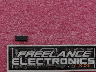
MAX3100EPD
Part #
MAX3100EPD
Description
SPI/MICROWIRE-COMPATIBLE UARTIN A QSOP-16 P - Bulk
Category
IC
Availability
In Stock
Qty
5
Manufacturer
Available
Qty
MAXIM
Date Code: 9813
Freelance Stock:
5
Ships Immediately
Request For Quote
Request For Quote
Related Items
MAXIM
IC
MAX3100CEE
$8.83663
MAXIM
IC
MAX310EWN
$29.42345
MAXIM
IC
MAX3110EENI
$7.74408
MAXIM
IC
MAX3111EENI
$8.85772
MAXIM
IC
MAX312FESE
$18.24512
MAXIM
IC
MAX3140EEI
$11.15670