SLUS198C – FEBUARY 2000 - REVISED - JUNE 2001
2
POST OFFICE BOX 655303 • DALLAS, TEXAS 75265
description (continued)
When the output current is below the fault level, the output MOSFET is switched on with a nominal ON resistance
of 0.15 Ω. When the output current exceeds the fault level, but is less than the maximum-sourcing level, the
output remains switched on, but the fault timer starts, charging CT. Once CT charges to a preset threshold, the
switch is turned off, and remains off for 50 times the programmed fault time. When the output current reaches
the maximum sourcing level, the MOSFET transitions from a switch to a constant current source.
The UCC3915 can be put into sleep mode, drawing only 100 µA of supply current. Other features include an
open-drain fault-output indicator, thermal shutdown, undervoltage lockout, 7-V to 15-V operation, and
low-thermal resistance SOIC and TSSOP power packages.
absolute maximum ratings over operating free-air temperature (unless otherwise noted)
†
VIN 15.5 V. . . . . . . . . . . . . . . . . . . . . . . . . . . . . . . . . . . . . . . . . . . . . . . . . . . . . . . . . . . . . . . . . . . . . . . . . . . . . . . . . . . .
VOUT – VIN .0.3 V. . . . . . . . . . . . . . . . . . . . . . . . . . . . . . . . . . . . . . . . . . . . . . . . . . . . . . . . . . . . . . . . . . . . . . . . . . . . . .
FAULT
sink current 50 mA. . . . . . . . . . . . . . . . . . . . . . . . . . . . . . . . . . . . . . . . . . . . . . . . . . . . . . . . . . . . . . . . . . . . . . .
FAULT
voltage –0.3 V to 8 V. . . . . . . . . . . . . . . . . . . . . . . . . . . . . . . . . . . . . . . . . . . . . . . . . . . . . . . . . . . . . . . . . . . . .
Output current Self limiting. . . . . . . . . . . . . . . . . . . . . . . . . . . . . . . . . . . . . . . . . . . . . . . . . . . . . . . . . . . . . . . . . . . . . . .
TTL input voltage –0.3 to VIN. . . . . . . . . . . . . . . . . . . . . . . . . . . . . . . . . . . . . . . . . . . . . . . . . . . . . . . . . . . . . . . . . . . .
Storage temperature, T
stg
–65°C to 150°C. . . . . . . . . . . . . . . . . . . . . . . . . . . . . . . . . . . . . . . . . . . . . . . . . . . . . . . . .
Junction temperature, T
J
–55°C to 150°C. . . . . . . . . . . . . . . . . . . . . . . . . . . . . . . . . . . . . . . . . . . . . . . . . . . . . . . . . .
Lead temperature (soldering, 10 sec.) 300°C. . . . . . . . . . . . . . . . . . . . . . . . . . . . . . . . . . . . . . . . . . . . . . . . . . . . . .
†
Stresses beyond those listed under “absolute maximum ratings” may cause permanent damage to the device. These are stress ratings only, and
functional operation of the device at these or any other conditions beyond those indicated under “recommended operating conditions” is not
implied. Exposure to absolute-maximum-rated conditions for extended periods may affect device reliability.
‡
Currents are positive into, negative out of the specified terminal. Consult Packaging Section of the Interface Products Data Book (TI Literature
Number SLUD002) for thermal limitations and considerations of packages.
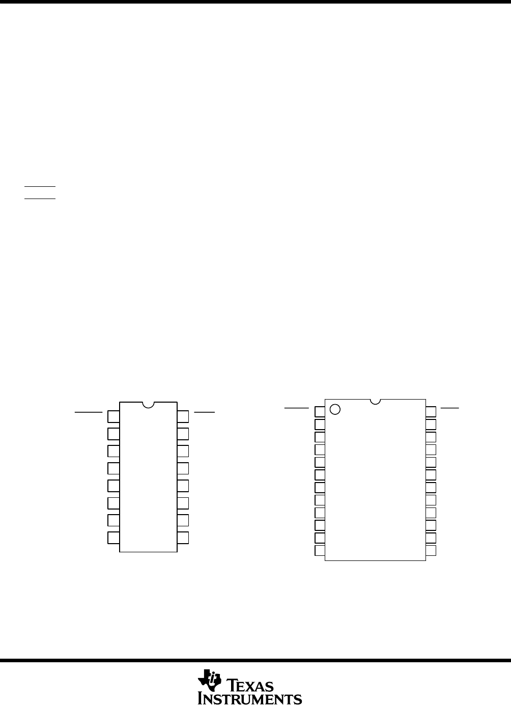
package information
DIL-16, SOIC-16
N, DP Package
(TOP VIEW)
TSSOP-24,
PWP Package
(TOP VIEW)
*Pin 5 serves as lowest impedance to the electrical
ground; Pins 4, 12, and 13 serve as heat sink/ground.
These pins should be connected to large etch areas to
help dissipate heat. For N Package, pins 4, 12, and 13
are N/C.
*Pin 9 serves as lowest impedance to the electrical ground;
other GND pins serve as heat sink/ground. These pins should
be connected to large etch areas to help dissipate heat.
B3
N/C
N/C
GND*
GND*
FAULT
VIN
EGND*
GND*
GND*
VIN
N/C
GND*
SHTDWN
GND*
B2
GND*
GND*
CT
12
11
10
9
8
7
6
5
4
3
2
1
13
14
15
16
17
18
19
20
21
22
23
24
IMAX
VOUT
VOUT
B1 B0
FAULT16
15
14
13
12
11
10
9
1
2
3
4
5
6
7
8
VOUT
VOUT
GND*
GND*
CT
IMAX
B0
SHTDWN
VIN
VIN
GND*
EGND*
B3
B2
B1


