Freelance Electronics Components Distributor
Closed Dec 25th-26th
800-300-1968
We Stock Hard to Find Parts

TPA0172PWP

Part # TPA0172PWP
Description STEREO 2W AUDIO AMP
Category IC
Availability In Stock
Qty 33
Qty Price
1 - 6 $8.37375
7 - 13 $6.66094
14 - 20 $6.28031
21 - 27 $5.83625
28 + $5.20188
Manufacturer Available Qty
Texas Instruments
Date Code: 0422
  • Shipping Freelance Stock: 33
    Ships Immediately


Technical Document


DISCLAIMER: The information provided herein is solely for informational purposes. Customers must be aware of the suitability of this product for their application, and consider that variable factors such as Manufacturer, Product Category, Date Codes, Pictures and Descriptions may differ from available inventory.

TPA0172
2-W STEREO AUDIO POWER AMPLIFIER
WITH I
2
C BUS
SLOS327C – AUGUST 2000 – REVISED MAY 2001
1
POST OFFICE BOX 655303 DALLAS, TEXAS 75265
I
2
C Bus Controllable
2-W/Ch Output Power Into 4- Load
Low Supply Current and Shutdown Current
Depop Circuitry
Digital Volume Control From 20 dB to
–60 dB
Internal Gain Control, Which Eliminates
External Gain-Setting Resistors
Fully Differential Input
Stereo Input MUX
PC-Beep Input
Compatible With PC 99 Desktop Line-Out
Into 10-k Load
Compatible With PC 99 Portable Into 8-
Load
Surface-Mount Power Packaging
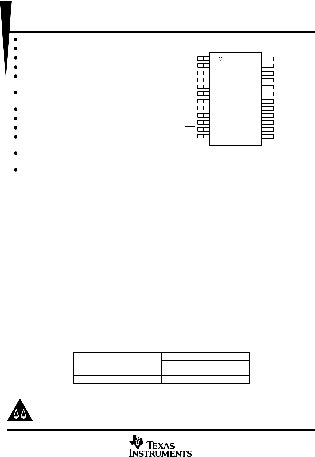
24-Pin TSSOP PowerPAD
description
The TPA0172 is a stereo audio power amplifier in a 24-pin TSSOP thermally enhanced package capable of
delivering 2 W of continuous RMS power per channel into 4- loads. This device utilizes the I
2
C bus to control
its functionality, which minimizes the number of external components needed, simplifies the design, and frees
up board space for other features. When driving 1 W into 8- speakers, the TPA0172 has less than 0.2% THD+N
from 20 Hz to 20 kHz.
Included within this device is integrated depop circuitry that virtually eliminates transients that cause noise in
the speakers at power up, power down, and while transitioning in and out of shutdown mode.
The overall gain of the amplifier is controlled digitally by the volume control registers which are programmed
via the I
2
C interface. At power up, the amplifier defaults to –60 dB in BTL mode, or –66 dB in SE mode. There
are four registers that contain the gains: left BTL, right BTL, left SE, and right SE. Each register contains six bits,
which allows 64 gain steps from –60 dB to 20 dB in 1.25-dB steps, and two bits that mute the amplifier.
The TPA0172 only consumes 6.5 mA of supply current during normal operation. A shutdown mode is included
that reduces supply current to less than 15 µA.
The PowerPAD package (PWP) delivers a level of thermal performance that was previously achievable on
TO-200-type packages. Thermal impedances of approximately 35°C/W are truly realized in multilayer PCB
applications. This allows the TPA0172 to operate at full power into 8- loads at ambient temperatures of 85°C.
AVAILABLE OPTIONS
PACKAGED DEVICE
T
A
TSSOP
(PWP)
–40°C to 85°C TPA0172PWP
The PWP package is available taped and reeled. To order a taped and reeled part,
add the suffix R to the part number (e.g., TPA0172PWPR).
Please be aware that an important notice concerning availability, standard warranty, and use in critical applications of
Texas Instruments semiconductor products and disclaimers thereto appears at the end of this data sheet.
Copyright 2001, Texas Instruments Incorporated
PRODUCTION DATA information is current as of publication date.
Products conform to specifications per the terms of Texas Instruments
standard warranty. Production processing does not necessarily include
testing of all parameters.
1
2
3
4
5
6
7
8
9
10
11
12
24
23
22
21
20
19
18
17
16
15
14
13
GND
LOUT+
PC-BEEP
ADDRESS0
LIN
LLINEIN
LHPIN
PV
DD
RIN
ADDRESS1
SE/BTL
ROUT+
LOUT–
SCL
SHUTDOWN
BYPASS
V
DD
PV
DD
RLINEIN
RHPIN
I2CV
DD
SDA
ROUT–
GND
PWP PACKAGE
(TOP VIEW)
PowerPAD is a trademark of Texas Instruments.
TPA0172
2-W STEREO AUDIO POWER AMPLIFIER
WITH I
2
C BUS
SLOS327C AUGUST 2000 REVISED MAY 2001
2
POST OFFICE BOX 655303 DALLAS, TEXAS 75265
functional block diagram
ROUT+
+
+
R
MUX
64-Step
Volume
Control
PC-
Beep
MUX
Control
Depop
Circuitry
Power
Management
+
+
L
MUX
64-Step
Volume
Control
RHPIN
RLINEIN
RIN
PC-BEEP
SE/BTL
LHPIN
LLINEIN
LIN
ROUT
PV
DD
V
DD
BYPASS
SHUTDOWN
GND
LOUT+
LOUT
I
2
C
CONTROL
ADDRESS0
ADDRESS1
SCL
SDA
I2CV
DD
TPA0172
2-W STEREO AUDIO POWER AMPLIFIER
WITH I
2
C BUS
SLOS327C AUGUST 2000 REVISED MAY 2001
3
POST OFFICE BOX 655303 DALLAS, TEXAS 75265
Terminal Functions
TERMINAL
I/O
DESCRIPTION
NAME NO.
I/O
DESCRIPTION
ADDRESS0 4 I Bit 0 of user-setable portion of devices I
2
C address.
ADDRESS1 10 I Bit 1 of user-setable portion of devices I
2
C address.
BYPASS 21 Tap to voltage divider for internal midsupply bias generator.
GND 1, 13 Ground connection for circuitry. Connect to thermal pad
LHPIN 7 I Left-channel headphone input, selected when SE/BTL is held high, or programmed via I
2
C.
LIN 5 I Common left input for fully differential input. AC ground for single-ended inputs.
LLINEIN 6 I Left-channel line input, selected when SE/BTL is held low, or programmed via I
2
C.
LOUT+ 2 O Left-channel positive output in BTL mode, and positive output in SE mode.
LOUT 24 O Left-channel negative output in BTL mode, and high impedance in SE mode.
PC-BEEP 3 I The input for PC-BEEP mode which is enabled when a > 1-V (peak-to-peak) square wave is input to this
terminal, when PCB ENABLE is held high, or programmed via I
2
C. If not used, ground this terminal.
I2CV
DD
16 I The voltage on this terminal sets the trip points for the I
2
C interface. If the system I
2
C bus is running at 3.3 V,
then tie this terminal to 3.3 V. If the system I
2
C bus is running at 5 V, then tie this terminal to 5 V.
PV
DD
8, 19 I Power supply
RHPIN 17 I Right-channel headphone input, selected when SE/BTL is held high, or programmed via I
2
C.
RIN 9 I Common right input for fully differential input. AC ground for single-ended inputs.
RLINEIN 18 I Right-channel line input, selected when SE/BTL is held low, or programmed via I
2
C.
ROUT+ 12 O Right-channel positive output in BTL mode, and positive output in SE mode.
ROUT 14 O Right-channel negative output in BTL mode, and high impedance in SE mode.
SCL 23 I I
2
C clock line
SDA 15 Serial data line of the I
2
C bus. Pullup resistor must comply with the I
2
C standard: minimum value = 3 k,
maximum value = 19 k. Pull up to I2CV
DD
SE/BTL 11 I Input MUX control input. When this terminal is held high, the LHPIN or RHPIN, and the SE output are
selected. When this terminal is held low, the LLINEIN or RLINEIN, and the BTL
output are selected. This
functionality can also be programmed via I
2
C.
SHUTDOWN 22 I When held low, this terminal places the device in the shutdown mode, except for the PC-BEEP input and the
I
2
C bus.
V
DD
20 I Power supply
1234567NEXT