SN54LS240, SN54LS241, SN54LS244, SN54S240, SN54S241, SN54S244
SN74LS240, SN74LS241, SN74LS244, SN74S240, SN74S241, SN74S244
OCTAL BUFFERS AND LINE DRIVERS WITH 3-STATE OUTPUTS
SDLS144B – APRIL 1985 – REVISED FEBRUARY 2002
10
POST OFFICE BOX 655303 • DALLAS, TEXAS 75265
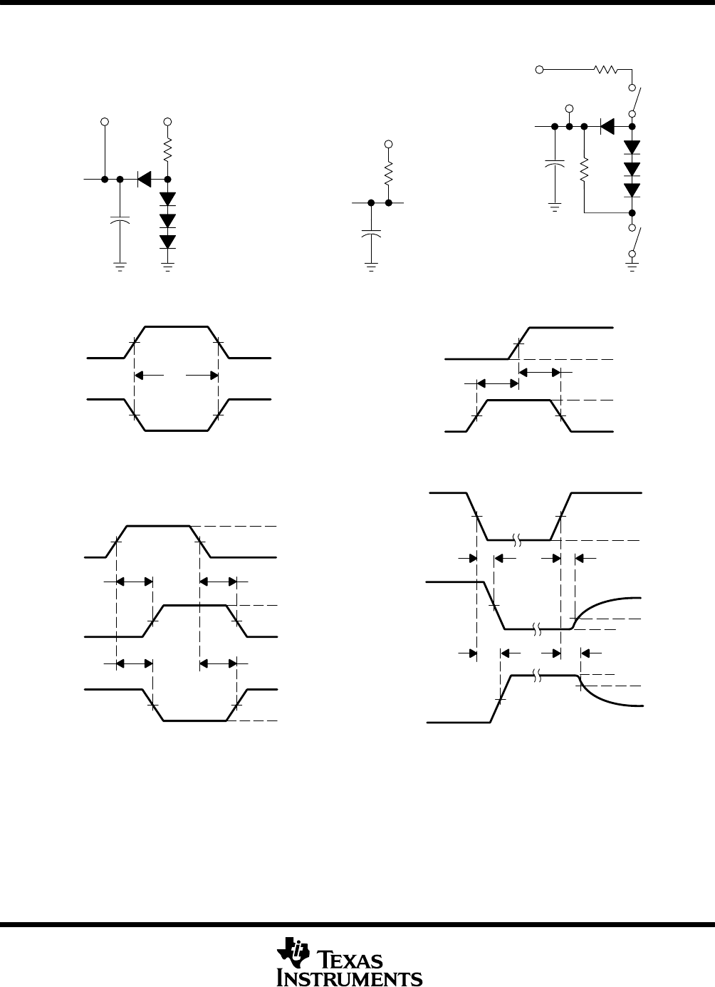
PARAMETER MEASUREMENT INFORMATION
SERIES 54LS/74LS DEVICES
t
PHL
t
PLH
t
PLH
t
PHL
LOAD CIRCUIT
FOR 3-STATE OUTPUTS
High-Level
Pulse
Low-Level
Pulse
VOLTAGE WAVEFORMS
PULSE DURATIONS
Input
Out-of-Phase
Output
(see Note D)
3 V
0 V
V
OL
V
OH
V
OH
V
OL
In-Phase
Output
(see Note D)
VOLTAGE WAVEFORMS
PROPAGATION DELAY TIMES
V
CC
R
L
Test
Point
From Output
Under Test
C
L
(see Note A)
LOAD CIRCUIT
FOR OPEN-COLLECTOR OUTPUTS
LOAD CIRCUIT
FOR 2-STATE TOTEM-POLE OUTPUTS
(see Note B)
V
CC
R
L
From Output
Under Test
C
L
(see Note A)
Test
Point
(see Note B)
V
CC
R
L
From Output
Under Test
C
L
(see Note A)
Test
Point
5 kΩ
NOTES: A. C
L
includes probe and jig capacitance.
B. All diodes are 1N3064 or equivalent.
C. Waveform 1 is for an output with internal conditions such that the output is low except when disabled by the output control.
Waveform 2 is for an output with internal conditions such that the output is high except when disabled by the output control.
D. S1 and S2 are closed for t
PLH
, t
PHL
, t
PHZ
, and t
PLZ
; S1 is open and S2 is closed for t
PZH
; S1 is closed and S2 is open for t
PZL
.
E. Phase relationships between inputs and outputs have been chosen arbitrarily for these examples.
F. All input pulses are supplied by generators having the following characteristics: PRR ≤ 1 MHz, Z
O
≈ 50 Ω, t
r
≤ 15 ns, t
f
≤ 6 ns.
G. The outputs are measured one at a time with one input transition per measurement.
S1
S2
t
PHZ
t
PLZ
t
PZL
t
PZH
3 V
3 V
0 V
0 V
t
h
t
su
VOLTAGE WAVEFORMS
SETUP AND HOLD TIMES
Timing
Input
Data
Input
3 V
0 V
Output
Control
(low-level
enabling)
Waveform 1
(see Notes C
and D)
Waveform 2
(see Notes C
and D)
≈1.5 V
V
OH
– 0.3 V
V
OL
+ 0.3 V
≈1.5 V
VOLTAGE WAVEFORMS
ENABLE AND DISABLE TIMES, 3-STATE OUTPUTS
1.3 V 1.3 V
1.3 V 1.3 V
1.3 V
1.3 V 1.3 V
1.3 V 1.3 V
1.3 V
1.3 V
t
w
1.3 V 1.3 V
1.3 V 1.3 V
1.3 V 1.3 V
V
OL
V
OH
Figure 1. Load Circuits and Voltage Waveforms