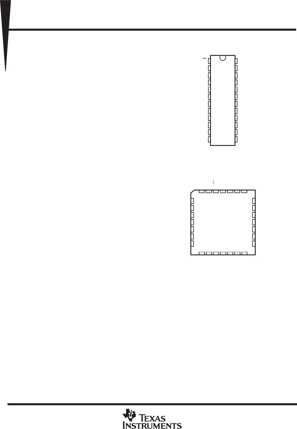
SN54AS885 . . . JT PACKAGE
SN74AS885 . . . DW OR NT PACKAGE
(TOP VIEW)
SN54AS885 . . . FK PACKAGE
(TOP VIEW)
1
2
3
4
5
6
7
8
9
10
11
12
24
23
22
21
20
19
18
17
16
15
14
13
L/A
P < QIN
P > QIN
Q7
Q6
Q5
Q4
Q3
Q2
Q1
Q0
GND
V
CC
PLE
P7
P6
P5
P4
P3
P2
P1
P0
P < QOUT
P > QOUT
NC – No internal connection
3212827
12 13
5
6
7
8
9
10
11
25
24
23
22
21
20
19
P6
P5
P4
NC
P3
P2
P1
Q7
Q6
Q5
NC
Q4
Q3
Q2
426
14 15 16 17 18
Q1
Q0
GND
NC
P > QOUT
P < QOUT
P0
P > QIN
P < QIN
L/A
NC
PLE
P7
V
CC
SN54AS885, SN74AS885
8-BIT MAGNITUDE COMPARATORS
SDAS236A – DECEMBER 1982 – REVISED JANUARY 1995
Copyright 1995, Texas Instruments Incorporated
1
POST OFFICE BOX 655303 • DALLAS, TEXAS 75265
• Latchable P-Input Ports With Power-Up
Clear
• Choice of Logical or Arithmetic
(Two’s Complement) Comparison
• Data and PLE Inputs Utilize pnp Input
Transistors to Reduce dc Loading Effects
• Approximately 35% Improvement in
ac Performance Over Schottky TTL While
Performing More Functions
• Cascadable to n Bits While Maintaining
High Performance
• 10% Less Power Than STTL for an 8-Bit
Comparison
• Package Options Include Plastic
Small-Outline (DW) Packages, Ceramic
Chip Carriers (FK), and Standard Plastic
(NT) and Ceramic (JT) 300-mil DIPs
description
These advanced Schottky devices are capable of
performing high-speed arithmetic or logic
comparisons on two 8-bit binary or two’s
complement words. Two fully decoded decisions
about words P and Q are externally available at
two outputs. These devices are fully expandable
to any number of bits without external gates. To
compare words of longer lengths, the P > QOUT
and P < QOUT outputs of a stage handling less
significant bits can be connected to the P > QIN
and P < QIN inputs of the next stage handling
more significant bits. The cascading paths are
implemented with only a two-gate-level delay to
reduce overall comparison times for long words.
Two alternative methods of cascading are shown
in
application information
.
The latch is transparent when P latch-enable
(PLE) input is high; the P-input port is latched
when PLE is low. This provides the designer with temporary storage for the P-data word. The enable circuitry
is implemented with minimal delay times to enhance performance when cascaded for longer words. The PLE,
P, and Q data inputs utilize pnp input transistors to reduce the low-level current input requirement to typically
–0.25 mA, which minimizes dc loading effects.
The SN54AS885 is characterized for operation over the full military temperature range of –55°C to 125°C. The
SN74AS885 is characterized for operation from 0°C to 70°C.
PRODUCTION DATA information is current as of publication date.
Products conform to specifications per the terms of Texas Instruments
standard warranty. Production processing does not necessarily include
testing of all parameters.


