Freelance Electronics Components Distributor
Closed Dec 25th-26th
800-300-1968
We Stock Hard to Find Parts

SNJ54ALS38BW

Part # SNJ54ALS38BW
Description NAND Gate 4-Element 2-IN Bipolar 14-Pin CFPAK Tube
Category IC
Availability In Stock
Qty 9
Qty Price
1 - 1 $10.71477
2 - 3 $8.52311
4 - 5 $8.03608
6 - 7 $7.46787
8 + $6.65615
Manufacturer Available Qty
Texas Instruments
  • Shipping Freelance Stock: 9
    Ships Immediately


Technical Document


DISCLAIMER: The information provided herein is solely for informational purposes. Customers must be aware of the suitability of this product for their application, and consider that variable factors such as Manufacturer, Product Category, Date Codes, Pictures and Descriptions may differ from available inventory.

SN54ALS38B, SN74ALS38B
QUADRUPLE 2-INPUT POSITIVE-NAND BUFFERS
WITH OPEN-COLLECTOR OUTPUTS
SDAS196B – APRIL 1982 – REVISED DECEMBER 1994
Copyright 1994, Texas Instruments Incorporated
1
POST OFFICE BOX 655303 DALLAS, TEXAS 75265
Package Options Include Plastic
Small-Outline (D) Packages, Ceramic Chip
Carriers (FK), and Standard Plastic (N) and
Ceramic (J) 300-mil DIPs
description
These devices contain four independent 2-input
positive-NAND buffers with open-collector
outputs. They perform the Boolean functions
Y = A
B or Y = A + B in positive logic. The
open-collector outputs require pullup resistors to
perform correctly. These outputs may be
connected to other open-collector outputs to
implement active-low wired-OR or active-high
wired-AND functions. Open-collector devices
often are used to generate higher V
OH
levels.
The SN54ALS38B is characterized for operation
over the full military temperature range of –55°C
to 125°C. The SN74ALS38B is characterized for
operation from 0°C to 70°C.
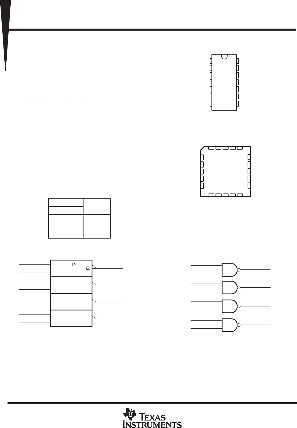
FUNCTION TABLE
(each gate)
INPUTS
OUTPUT
A B
Y
H H L
L XH
XLH
logic symbol
logic diagram (positive logic)
1
1A
2
1B
4
2A
5
2B
9
3A
10
3B
12
4A
13
4B
1Y
3
2Y
6
3Y
8
4Y
11
&
1
1A
2
1B
4
2A
5
2B
9
3A
10
3B
12
4A
13
4B
1Y
3
2Y
6
3Y
8
4Y
11
This symbol is in accordance with ANSI/IEEE Std 91-1984 and
IEC Publication 617-12.
Pin numbers shown are for the D, J, and N packages.
SN54ALS38B ...J PACKAGE
SN74ALS38B ...D OR N PACKAGE
(TOP VIEW)
1
2
3
4
5
6
7
14
13
12
11
10
9
8
1A
1B
1Y
2A
2B
2Y
GND
V
CC
4B
4A
4Y
3B
3A
3Y
SN54ALS38B . . . FK PACKAGE
(TOP VIEW)
3212019
910111213
4
5
6
7
8
18
17
16
15
14
4A
NC
4Y
NC
3B
1Y
NC
2A
NC
2B
1B
1A
NC
3Y
3A
V
4B
2Y
NC
CC
NC – No internal connection
GND
PRODUCTION DATA information is current as of publication date.
Products conform to specifications per the terms of Texas Instruments
standard warranty. Production processing does not necessarily include
testing of all parameters.
SN54ALS38B, SN74ALS38B
QUADRUPLE 2-INPUT POSITIVE-NAND BUFFERS
WITH OPEN-COLLECTOR OUTPUTS
SDAS196B – APRIL 1982 – REVISED DECEMBER 1994
2
POST OFFICE BOX 655303 DALLAS, TEXAS 75265
absolute maximum ratings over operating free-air temperature range (unless otherwise noted)
Supply voltage, V
CC
7 V. . . . . . . . . . . . . . . . . . . . . . . . . . . . . . . . . . . . . . . . . . . . . . . . . . . . . . . . . . . . . . . . . . . . . . . .
Input voltage, V
I
7 V. . . . . . . . . . . . . . . . . . . . . . . . . . . . . . . . . . . . . . . . . . . . . . . . . . . . . . . . . . . . . . . . . . . . . . . . . . . .
Operating free-air temperature range, T
A
: SN54ALS38B 55°C to 125°C. . . . . . . . . . . . . . . . . . . . . . . . . . . . .
SN74ALS38B 0°C to 70°C. . . . . . . . . . . . . . . . . . . . . . . . . . . . . . . . .
Storage temperature range 65°C to 150°C. . . . . . . . . . . . . . . . . . . . . . . . . . . . . . . . . . . . . . . . . . . . . . . . . . . . . . .
Stresses beyond those listed under “absolute maximum ratings” may cause permanent damage to the device. These are stress ratings only, and
functional operation of the device at these or any other conditions beyond those indicated under “recommended operating conditions” is not
implied. Exposure to absolute-maximum-rated conditions for extended periods may affect device reliability.
recommended operating conditions
SN54ALS38B SN74ALS38B
UNIT
MIN NOM MAX MIN NOM MAX
UNIT
V
CC
Supply voltage 4.5 5 5.5 4.5 5 5.5 V
V
IH
High-level input voltage 2 2 V
V
IL
Low-level input voltage 0.7 0.8 V
V
OH
High-level output voltage 5.5 5.5 V
I
OL
Low-level output current 12 24 mA
T
A
Operating free-air temperature –55 125 0 70 °C
electrical characteristics over recommended operating free-air temperature range (unless
otherwise noted)
PARAMETER
TEST CONDITIONS
SN54ALS38B SN74ALS38B
UNIT
PARAMETER
TEST
CONDITIONS
MIN TYP
MAX MIN TYP
MAX
UNIT
V
IK
V
CC
= 4.5 V, I
I
= –18 mA –1.5 –1.5 V
V
OL
V
CC
=45V
I
OL
= 12 mA 0.25 0.4 0.25 0.4
V
V
OL
V
CC
=
4
.
5
V
I
OL
= 24 mA 0.35 0.5
V
I
I
V
CC
= 5.5 V, V
I
= 7 V 0.1 0.1 mA
I
IH
V
CC
= 5.5 V, V
I
= 2.7 V 20 20 µA
I
IL
V
CC
= 5.5 V, V
I
= 0.4 V 0.1 0.1 mA
I
OH
V
CC
= 4.5 V, V
OH
= 5.5 V 0.1 0.1 mA
I
CCH
V
CC
= 5.5 V, V
I
= 0 0.86 1.6 0.86 1.6 mA
I
CCL
V
CC
= 5.5 V, V
I
= 4.5 V 4.8 7.8 4.8 7.8 mA
All typical values are at V
CC
= 5 V, T
A
= 25°C.
switching characteristics (see Figure 1)
PARAMETER
FROM
(
INPUT
)
TO
(
OUTPUT
)
V
CC
= 4.5 V to 5.5 V,
C
L
= 50 pF,
R
L
= 500 ,
T
A
= MIN to MAX
§
UNIT
(INPUT)
(OUTPUT)
SN54ALS38B SN74ALS38B
MIN MAX MIN MAX
t
PLH
AorB
Y
7 59 10 33
ns
t
PHL
A
or
B
Y
2 20 1 12
ns
§
For conditions shown as MIN or MAX, use the appropriate value specified under recommended operating conditions.
SN54ALS38B, SN74ALS38B
QUADRUPLE 2-INPUT POSITIVE-NAND BUFFERS
WITH OPEN-COLLECTOR OUTPUTS
SDAS196B – APRIL 1982 – REVISED DECEMBER 1994
3
POST OFFICE BOX 655303 DALLAS, TEXAS 75265
PARAMETER MEASUREMENT INFORMATION
SERIES 54ALS/74ALS AND 54AS/74AS DEVICES
t
PHZ
t
PLZ
t
PHL
t
PLH
0.3 V
t
PZL
t
PZH
t
PLH
t
PHL
LOAD CIRCUIT
FOR 3-STATE OUTPUTS
From Output
Under Test
Test
Point
R1
S1
C
L
(see Note A)
7 V
1.3 V
1.3 V1.3 V
3.5 V
3.5 V
0.3 V
0.3 V
t
h
t
su
VOLTAGE WAVEFORMS
SETUP AND HOLD TIMES
Timing
Input
Data
Input
1.3 V 1.3 V
3.5 V
3.5 V
0.3 V
0.3 V
High-Level
Pulse
Low-Level
Pulse
t
w
VOLTAGE WAVEFORMS
PULSE DURATIONS
Input
Out-of-Phase
Output
(see Note C)
1.3 V 1.3 V
1.3 V1.3 V
1.3 V 1.3 V
1.3 V1.3 V
1.3 V
1.3 V
3.5 V
3.5 V
0.3 V
0.3 V
V
OL
V
OH
V
OH
V
OL
Output
Control
(low-level
enabling)
Waveform 1
S1 Closed
(see Note B)
Waveform 2
S1 Open
(see Note B)
0 V
V
OH
V
OL
3.5 V
In-Phase
Output
0.3 V
1.3 V 1.3 V
VOLTAGE WAVEFORMS
PROPAGATION DELAY TIMES
VOLTAGE WAVEFORMS
ENABLE AND DISABLE TIMES, 3-STATE OUTPUTS
R2
V
CC
R
L
Test
Point
From Output
Under Test
C
L
(see Note A)
LOAD CIRCUIT
FOR OPEN-COLLECTOR OUTPUTS
LOAD CIRCUIT FOR
BI-STATE
TOTEM-POLE OUTPUTS
From Output
Under Test
Test
Point
C
L
(see Note A)
R
L
R
L
= R1 = R2
NOTES: A. C
L
includes probe and jig capacitance.
B. Waveform 1 is for an output with internal conditions such that the output is low except when disabled by the output control.
Waveform 2 is for an output with internal conditions such that the output is high except when disabled by the output control.
C. When measuring propagation delay items of 3-state outputs, switch S1 is open.
D. All input pulses have the following characteristics: PRR 1 MHz, t
r
= t
f
= 2 ns, duty cycle = 50%.
E. The outputs are measured one at a time with one transition per measurement.
Figure 1. Load Circuits and Voltage Waveforms
123456NEXT