Closed Dec 25th-26th
800-300-1968
We Stock Hard to Find Parts
My Account
|
My Orders
|
My Cart
Questions?
(800) 300-1968
Register
(current)
My Account
(current)
My Orders
(current)
My Cart
(current)
Categories
(current)
Manufacturers
Request a Quote
Sell Your Excess
Consignment
Quality Assurance
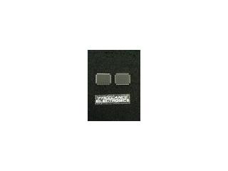
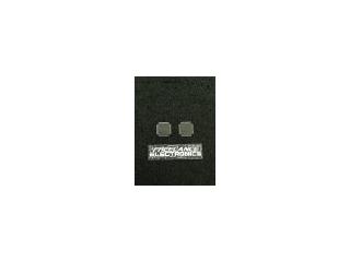
DP83847ALQA56A
Part #
DP83847ALQA56A
Description
IC ETHERNET TRANSCEIVER 56WQFN
Category
IC
Availability
In Stock
Qty
4
Qty
Price
1 +
$3.46100
Manufacturer
Available
Qty
National Semiconductor Corp
Freelance Stock:
4
Ships Immediately
Add to Cart
Related Items
National Semiconductor Corp
IC
DP83840AVCE
$1.60170
National Semiconductor Corp
IC
DP83843BVJE
$15.81821
National Semiconductor Corp
IC
DP83846AVHG
$6.85060
National Semiconductor Corp
IC
DP83848JSQ/NOPB
$1.30200
Fairchild Semiconductor
IC
008-25424
$11.58351
Harris Corporation
IC
01-6945-9