Freelance Electronics Components Distributor
Closed Dec 25th-26th
800-300-1968
We Stock Hard to Find Parts

OP297EZ

Part # OP297EZ
Description OP AMP DUAL GP 20V 8CDIP - Rail/Tube
Category IC
Availability Out of Stock
Qty 0
Qty Price
1 + $9.13760


Technical Document


DISCLAIMER: The information provided herein is solely for informational purposes. Customers must be aware of the suitability of this product for their application, and consider that variable factors such as Manufacturer, Product Category, Date Codes, Pictures and Descriptions may differ from available inventory.

8/21/97 4:00 PM
REV. D
Information furnished by Analog Devices is believed to be accurate and
reliable. However, no responsibility is assumed by Analog Devices for its
use, nor for any infringements of patents or other rights of third parties
which may result from its use. No license is granted by implication or
otherwise under any patent or patent rights of Analog Devices.
a
OP297
One Technology Way, P.O. Box 9106, Norwood, MA 02062-9106, U.S.A.
Tel: 617/329-4700 World Wide Web Site: http://www.analog.com
Fax: 617/326-8703 © Analog Devices, Inc., 1997
Dual Low Bias Current
Precision Operational Amplifier
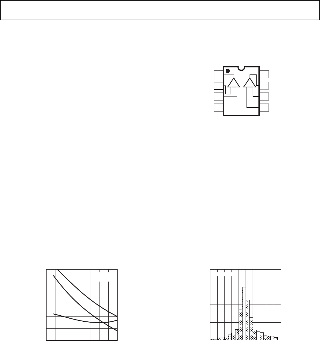
PIN CONNECTIONS
Plastic Epoxy-DIP (P Suffix)
8-Pin Cerdip (Z Suffix)
8-Pin Narrow Body SOIC (S Suffix)
FEATURES
Precision Performance in Standard SO-8 Pinout
Low Offset Voltage: 50 V max
Low Offset Voltage Drift: 0.6 V/C max
Very Low Bias Current:
␣ +25C (100 pA max)
␣␣–55C to +125C (450 pA max)
Very High Open-Loop Gain (2000 V/mV min)
Low Supply Current (Per Amplifier): 625 A max
Operates From 62 V to 620 V Supplies
High Common-Mode Rejection: 120 dB min
Pin Compatible to LT1013, AD706, AD708, OP221,
␣ LM158, and MC1458/1558 with Improved Performance
APPLICATIONS
Strain Gauge and Bridge Amplifiers
High Stability Thermocouple Amplifiers
Instrumentation Amplifiers
Photo-Current Monitors
High-Gain Linearity Amplifiers
Long-Term Integrators/Filters
Sample-and-Hold Amplifiers
Peak Detectors
Logarithmic Amplifiers
Battery-Powered Systems
GENERAL DESCRIPTION
The OP297 is the first dual op amp to pack precision perfor-
mance into the space-saving, industry standard 8-pin SO pack-
age. Its combination of precision with low power and extremely
low input bias current makes the dual OP297 useful in a wide
variety of applications.
Precision performance of the OP297 includes very low offset,
under 50 µV, and low drift, below 0.6 µV/°C. Open-loop gain
exceeds 2000 V/mV insuring high linearity in every application.
Errors due to common-mode signals are eliminated by the
OP297’s common-mode rejection of over 120 dB. The
OP297’s power supply rejection of over 120 dB minimizes
offset voltage changes experienced in battery powered systems.
Supply current of the OP297 is under 625 µA per amplifier and
it can operate with supply voltages as low as ±2 V.
The OP297 utilizes a super-beta input stage with bias current
cancellation to maintain picoamp bias currents at all tempera-
tures. This is in contrast to FET input op amps whose bias
currents start in the picoamp range at 25°C, but double for
every 10°C rise in temperature, to reach the nanoamp range
above 85°C. Input bias current of the OP 297 is under 100 pA
at 25°C and is under 450 pA over the military temperature
range.
Combining precision, low power and low bias current, the
OP297 is ideal for a number of applications including instru-
mentation amplifiers, log amplifiers, photodiode preamplifiers
and long-term integrators. For a single device, see the OP97;
for a quad, see the OP497.
Figure 1. Low Bias Current Over Temperature Figure 2. Very Low Offset
1
2
3
45
6
7
8
OUT A V+
–IN A OUT B
+IN A –IN B
V– +IN B
+
+
B
A
TEMPERATURE (°C)
INPUT CURRENT (pA)
60
40
20
0
20
–40
–60
–75 50 –25 0 25 50 75 100 125
V
S
= ±15V
V
CM
= 0V
I
B
I
B
+
I
OS
INPUT OFFSET VOLTAGE (µV)
NUMBER OF UNITS
400
300
200
100
0
–100 –80 –60 –40 –20 0 20 40 60 80 100
1200 UNITS
T
A
= +25°C
V
S
= ±15V
V
CM
= 0V
8/21/97 4:00 PM
–2–
REV. D
OP297–SPECIFICATIONS
ELECTRICAL CHARACTERISTICS
␣␣␣␣OP297A/E ␣␣␣␣ OP297F ␣␣␣␣␣ OP297G
Parameter Symbol Conditions Min Typ Max Min Typ Max Min Typ Max Units
Input Offset Voltage V
OS
25 50 50 100 80 200 µV
Long-Term Input
␣ ␣ Voltage Stability 0.1 0.1 0.1 µV/mo
Input Offset Current I
OS
V
CM
= 0 V 20 100 35 150 50 200 pA
Input Bias Current I
B
V
CM
= 0 V 20 ±100 35 ±150 50 ±200 pA
Input Noise Voltage e
n
p-p 0.1 Hz to 10 Hz 0.5 0.5 0.5 µV p-p
Input Noise e
n
f
O
= 10 Hz 20 20 20 nV/Hz
␣ ␣ Voltage Density e
n
f
O
= 1000 Hz 17 17 17 nV/Hz
Input Noise Current Density i
n
f
O
= 10 Hz 20 20 20 fAHz
Input Resistance
␣ ␣ Differential Mode R
IN
30 30 30 M
Input Resistance
␣ ␣ Common-Mode R
INCM
500 500 500 G
Large-Signal V
O
= ± 10 V
␣ ␣ Voltage Gain A
VO
R
L
= 2 k 2000 4000 1500 3200 1200 3200 V/mV
Input Voltage Range IVR (Note 1) ± 13 ±14 ±13 ±14 ±13 ±14 V
Common-Mode Rejection CMR V
CM
= ±13 V 120 140 114 135 114 135 dB
Power Supply Rejection PSR V
S
= ±2 V to ±20 V 120 130 114 125 114 125 dB
Output Voltage Swing V
O
R
L
= 10 kΩ±13 ±14 ±13 ±14 ±13 ±14 V
V
O
R
L
= 2 kΩ±13 ±13.7 ±13 ± 13.7 ±13 ± 13.7 V
Supply Current Per Amplifier I
SY
No Load 525 625 525 625 525 625 µA
Supply Voltage V
S
Operating Range ± 2 ±20 ± 2 ± 20 ±2 ±20 V
Slew Rate SR 0.05 0.15 0.05 0.15 0.05 0.15 V/µs
Gain Bandwidth Product GBWP A
V
= +1 500 500 500 kHz
Channel Separation CS V
O
= 20 V p–p 150 150 150 dB
f
O
= 10 Hz
Input Capacitance C
IN
333pF
NOTES
1
Guaranteed by CMR test.
Specifications subject to change without notice.
ELECTRICAL CHARACTERISTICS
␣␣␣␣␣ OP297A
Parameter Symbol Conditions Min Typ Max Units
Input Offset Voltage V
OS
45 100 µV
Average Input Offset Voltage Drift TCV
OS
0.2 0.6 µV/°C
Input Offset Current I
OS
V
CM
= 0 V 60 450 pA
Input Bias Current I
B
V
CM
= 0 V 60 ±450 pA
Large-Signal Voltage Gain A
VO
V
O
= ±10 V, R
L
= 2 k 1200 2700 V/mV
Input Voltage Range IVR (Note 1) ±13 ±13.5 V
Common-Mode Rejection CMR V
CM
= ±13 114 130 dB
Power Supply Rejection PSR V
S
= ±2.5 V to ±20 V 114 125 dB
Output Voltage Swing V
O
R
L
= 10 kΩ±13 ±13.4 V
Supply Current Per Amplifier I
SY
No Load 575 750 µA
Supply Voltage V
S
Operating Range ± 2.5 ±20 V
NOTES
1
Guaranteed by CMR test.
Specifications subject to change without notice.
(@ V
S
= 15 V, T
A
= +25C, unless otherwise noted.)
(@ V
S
= 15 V, –55C T
A
+125C for OP297A, unless otherwise noted.)
8/21/97 4:00 PM
–3–REV. D
OP297
ELECTRICAL CHARACTERISTICS
␣␣␣␣OP297E ␣␣␣␣ OP297F ␣␣␣␣␣ OP297G
Parameter Symbol Conditions Min Typ Max Min Typ Max Min Typ Max Units
Input Offset Voltage V
OS
35 100 80 300 110 400 µV
Average Input Offset
Voltage Drift TCV
OS
0.2 0.6 0.5 2.0 0.6 2.0 µV/°C
Input Offset Current I
OS
V
CM
= 0 V 50 450 80 750 80 750 pA
Input Bias Current I
B
V
CM
= 0 V 50 ±450 80 ±750 80 ±750 pA
Large-Signal Voltage Gain A
VO
V
O
= ±10 V,
R
L
= 2 k 1200 3200 1000 2500 700 2500 V/mV
Input Voltage Range IVR (Note 1) ±13 ±13.5 ±13 ±13.5 ±13 ±13.5 V
Common-Mode Rejection CMR V
CM
= ±13 114 130 108 130 108 130 dB
Power Supply Rejection PSR V
S
= ±2.5 V
to ±20 V 114 0.15 108 0.15 108 0.3 dB
Output Voltage Swing V
O
R
L
= 10 kΩ±13 ±13.4 ± 13 ±13.4 ± 13 ±13.4 V
Supply Current Per Amplifier I
SY
No Load 550 750 550 750 550 750 µA
Supply Voltage V
S
Operating Range ±2.5 ±20 ±2.5 ±20 ±2.5 ± 20 V
NOTES
1
Guaranteed by CMR test.
Specifications subject to change without notice.
(@ V
S
= 15 V, –40C T
A
+85C for OP297E/F/G, unless otherwise noted.)
Wafer Test Limits
Parameter Symbol Conditions Limit Units
Input Offset Voltage V
OS
200 µV max
Input Offset Current I
OS
V
CM
= 0 V 200 pA max
Input Bias Current I
B
V
CM
= 0 V ±200 pA max
Large-Signal Voltage Gain A
VO
V
O
= ±10 V, R
L
= 2 k 1200 V/mV min
Input Voltage Range IVR (Note 1) ±13 V min
Common-Mode Rejection CMR V
CM
= ±13 V 114 dB min
Power Supply PSR V
S
= ±2 V to ±l 8 V 114 dB min
Output Voltage Swing V
O
R
L
= 2 kΩ±13 V min
Supply Current Per Amplifier I
SY
No Load 625 µA max
NOTES
1. Guaranteed by CMR test.
Electrical tests are performed at wafer probe to the limits shown. Due to variations in assembly methods and normal yield loss, yield after packaging is not guaranteed
for standard product dice. Consult factory to negotiate specifications based on dice lot qualifications through sample lot assembly and testing.
(@ V
S
= 15 V, T
A
= +25C, unless otherwise noted.)
DICE CHARACTERISTICS
Dimension shown in inches and (mm).
Contact factory for latest dimensions
OUTPUT A
–INPUT A
+INPUT A
–V
S
0.074 (1.88)
+INPUT B
–INPUT B
OUTPUT B
+V
S
0.118 (3.00)
123456NEXT