Closed Dec 25th-26th
800-300-1968
We Stock Hard to Find Parts
My Account
|
My Orders
|
My Cart
Questions?
(800) 300-1968
Register
(current)
My Account
(current)
My Orders
(current)
My Cart
(current)
Categories
(current)
Manufacturers
Request a Quote
Sell Your Excess
Consignment
Quality Assurance
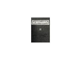
OP297GS
Part #
OP297GS
Description
DUAL LOW PWR PREC OP AMP
Category
IC
Availability
Out of Stock
Qty
0
Qty
Price
1 +
$2.09425
Related Items
Analog Devices
IC
OP297EZ
$9.13760
Analog Devices
IC
OP297F
Analog Devices
IC
OP297G
$8.85076
Fairchild Semiconductor
IC
008-25424
$11.58351
Harris Corporation
IC
01-6945-9
Motorola Corp
IC
010-143121-0002