Freelance Electronics Components Distributor
Closed Dec 25th-26th
800-300-1968
We Stock Hard to Find Parts

MSP430F2274TRHAT

Part # MSP430F2274TRHAT
Description MCU 16-bit MSP430 MSP430 RISC32KB Flash 2.5V/3.3V 40-Pin
Category IC
Availability In Stock
Qty 214
Qty Price
1 - 44 $3.57032
45 - 89 $2.84003
90 - 134 $2.67774
135 - 179 $2.48841
180 + $2.21793
Manufacturer Available Qty
Texas Instruments
Date Code: 0712
  • Shipping Freelance Stock: 16
    Ships Immediately
Texas Instruments
Date Code: 0706
  • Shipping Freelance Stock: 198
    Ships Immediately


Technical Document


DISCLAIMER: The information provided herein is solely for informational purposes. Customers must be aware of the suitability of this product for their application, and consider that variable factors such as Manufacturer, Product Category, Date Codes, Pictures and Descriptions may differ from available inventory.

MSP430x22x2, MSP430x22x4
MIXED SIGNAL MICROCONTROLLER
SLAS504B − JULY 2006 − REVISED JULY 2007
67
POST OFFICE BOX 655303 DALLAS, TEXAS 75265
POST OFFICE BOX 1443 HOUSTON, TEXAS 77251−1443
Port P2 pin schematic: P2.7, input/output with Schmitt trigger and crystal oscillator output
LFXT1 off
P2SEL.6
Bus
Keeper
EN
Direction
0: Input
1: Output
P2SEL.7
1
0
P2DIR.7
P2IN.7
P2IRQ.7
D
EN
Module X IN
1
0
Module X OUT
P2OUT.7
Interrupt
Edge
Select
Q
EN
Set
P2SEL.7
P2IES.7
P2IFG.7
P2IE.7
P2.7/XOUT
1
0
DVSS
DVCC
P2REN.7
Pad Logic
LFXT1 Oscillator
BCSCTL3.LFXT1Sx = 11
0
1
1
LFXT1CLK
From P2.6/XIN
P2.6/XIN
Port P2 (P2.7) pin functions
PIN NAME (P2 X)
X
FUNCTION
CONTROL BITS / SIGNALS
PIN NAME (P2.X)
X FUNCTION
P2DIR.x P2SEL.x
XOUT/P2.7 6 P2.7 (I/O) I: 0; O: 1 0
XOUT† (see Note 3) X 1
Default after reset (PUC/POR)
NOTES: 1. N/A: Not available or not applicable
2. X: Don’t care
3. If the pin XOUT/P2.7 is used as an input a current can flow until P2SEL.7 is cleared due to the oscillator output driver connection
to this pin after reset.
MSP430x22x2, MSP430x22x4
MIXED SIGNAL MICROCONTROLLER
SLAS504B − JULY 2006 − REVISED JULY 2007
68
POST OFFICE BOX 655303 DALLAS, TEXAS 75265
POST OFFICE BOX 1443 HOUSTON, TEXAS 77251−1443
Port P3 pin schematic: P3.0, input/output with Schmitt trigger
Bus
Keeper
EN
Direction
0: Input
1: Output
P3SEL.0
1
0
P3DIR.0
P3IN.0
D
EN
Module X IN
1
0
Module X OUT
P3OUT.0
P3.0/UC1STE/UC0CLK/A5
1
0
DVSS
DVCC
P3REN.0
ADC10AE0.5
Pad Logic
INCHx = 5
To ADC10
1
USCI Direction
Control
Port P3 (P3.0) pin functions
PIN NAME (P3 X)
X
Y
FUNCTION
CONTROL BITS / SIGNALS
PIN NAME (P3.X)
X Y FUNCTION
P3DIR.x P3SEL.x ADC10AE0.y
P3.0/ 0 5 P3.0† (I/O) I: 0; O: 1 0 0
UC1STE/UC0CLK/A5
UC1STE/UC0CLK (see Notes 3, 4) X 1 0
A5 (see Note 5) X X 1
Default after reset (PUC/POR)
NOTES: 1. N/A: Not available or not applicable
2. X: Don’t care
3. The pin direction is controlled by the USCI module.
4. UC0CLK function takes precedence over UC1STE function. If the pin is required as UC0CLK input or output USCI1 will be forced
to 3-wire SPI mode if 4-wire SPI mode is selected.
5. Setting the ADC10AE0.y bit disables the output driver as well as the input schmitt trigger to prevent parasitic cross currents when
applying analog signals.
MSP430x22x2, MSP430x22x4
MIXED SIGNAL MICROCONTROLLER
SLAS504B − JULY 2006 − REVISED JULY 2007
69
POST OFFICE BOX 655303 DALLAS, TEXAS 75265
POST OFFICE BOX 1443 HOUSTON, TEXAS 77251−1443
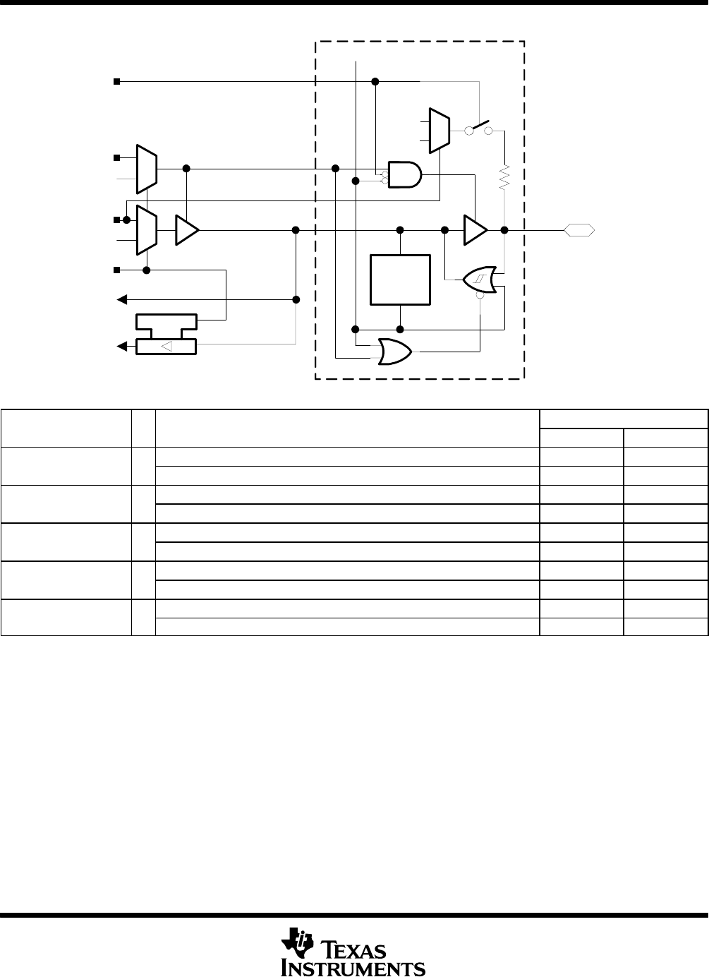
Port P3 pin schematic: P3.1 to P3.5, input/output with Schmitt trigger
Bus
Keeper
EN
Direction
0: Input
1: Output
P3SEL.x
1
0
P3DIR.x
P3IN.x
D
EN
Module X IN
1
0
Module X OUT
P3OUT.x
P3.1/UC1SIMO/UC1SCL
P3.2/UC1SOMI/UC1SDA
P3.3/UC1CLK/UC0STE
P3.4/UC0TXD/UC0SIMO
P3.5/UC0RXD/UC0SOMI
1
0
DVSS
DVCC
P3REN.x
Pad Logic
1
USCI Direction
Control
DVSS
Port P3 (P3.1 to P3.5) pin functions
PIN NAME (P3 X)
X
FUNCTION
CONTROL BITS / SIGNALS
PIN NAME (P3.X)
X FUNCTION
P3DIR.x P3SEL.x
P3.1/ 1 P3.1† (I/O) I: 0; O: 1 0
UC1SIMO/UC1SDA
UC1SIMO/UC1SDA (see Note 3) X 1
P3.2/ 1 P3.2† (I/O) I: 0; O: 1 0
UC1SOMI/UC1SCL
UC1SOMI/UC1SCL (see Note 3) X 1
P3.3/ 1 P3.3† (I/O) I: 0; O: 1 0
UC1CLK/UC0STE
UC1CLK/UC0STE (see Notes 3, 4) X 1
P3.4/ 1 P3.4† (I/O) I: 0; O: 1 0
UC0TXD/UC0SIMO
UC0TXD/UC0SIMO (see Note 3) X 1
P3.5/ 1 P3.5† (I/O) I: 0; O: 1 0
UC0RXD/UC0SOMI
UC0RXD/UC0SOMI (see Note 3) X 1
Default after reset (PUC/POR)
NOTES: 1. N/A: Not available or not applicable
2. X: Don’t care
3. The pin direction is controlled by the USCI module.
4. UC1CLK function takes precedence over UC0STE function. If the pin is required as UC1CLK input or output USCI0 will be forced
to 3-wire SPI mode even if 4-wire SPI mode is selected.
PREVIOUS1617181920212223242526272829NEXT