MSP430x22x2, MSP430x22x4
MIXED SIGNAL MICROCONTROLLER
SLAS504B − JULY 2006 − REVISED JULY 2007
55
POST OFFICE BOX 655303 • DALLAS, TEXAS 75265
POST OFFICE BOX 1443 • HOUSTON, TEXAS 77251−1443
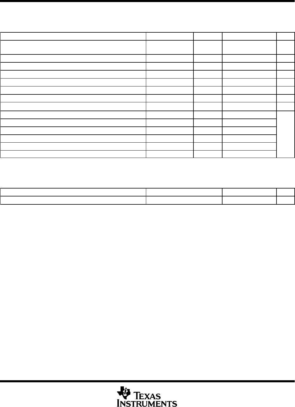
electrical characteristics over recommended ranges of supply voltage and operating free-air
temperature (unless otherwise noted) (continued)
Flash Memory
PARAMETER TEST CONDITIONS VCC MIN TYP MAX UNIT
V
CC(PGM/
ERASE)
Program and erase supply voltage 2.2 3.6 V
f
FTG
Flash timing generator frequency 257 476 kHz
I
PGM
Supply current from V
CC
during program 2.2 V/3.6 V 1 5 mA
I
ERASE
Supply current from V
CC
during erase 2.2 V/3.6 V 1 7 mA
t
CPT
Cumulative program time (see Note 1) 2.2 V/3.6 V 10 ms
t
CMErase
Cumulative mass erase time 2.2 V/3.6 V 20 ms
Program/erase endurance 10
4
10
5
cycles
t
Retention
Data retention duration T
J
= 25°C 100 years
t
Word
Word or byte program time see Note 2 30
t
Block,
0
Block program time for first byte or word see Note 2 25
t
Block,
1-63
Block program time for each additional byte or word see Note 2 18
t
Block,
End
Block program end-sequence wait time see Note 2 6
t
FTG
t
Mass
Erase
Mass erase time see Note 2 10593
t
Seg
Erase
Segment erase time see Note 2 4819
NOTES: 1. The cumulative program time must not be exceeded when writing to a 64-byte flash block. This parameter applies to all programming
methods: individual word/byte write and block write modes.
2. These values are hardwired into the flash controller’s state machine (t
FTG
= 1/f
FTG
).
RAM
PARAMETER TEST CONDITIONS MIN TYP MAX UNIT
V
(RAMh)
RAM retention supply voltage (see Note 1) CPU halted 1.6 V
NOTE 1: This parameter defines the minimum supply voltage V
CC
when the data in RAM remains unchanged. No program execution should
happen during this supply voltage condition.


