MSP430x22x2, MSP430x22x4
MIXED SIGNAL MICROCONTROLLER
SLAS504B − JULY 2006 − REVISED JULY 2007
48
POST OFFICE BOX 655303 • DALLAS, TEXAS 75265
POST OFFICE BOX 1443 • HOUSTON, TEXAS 77251−1443
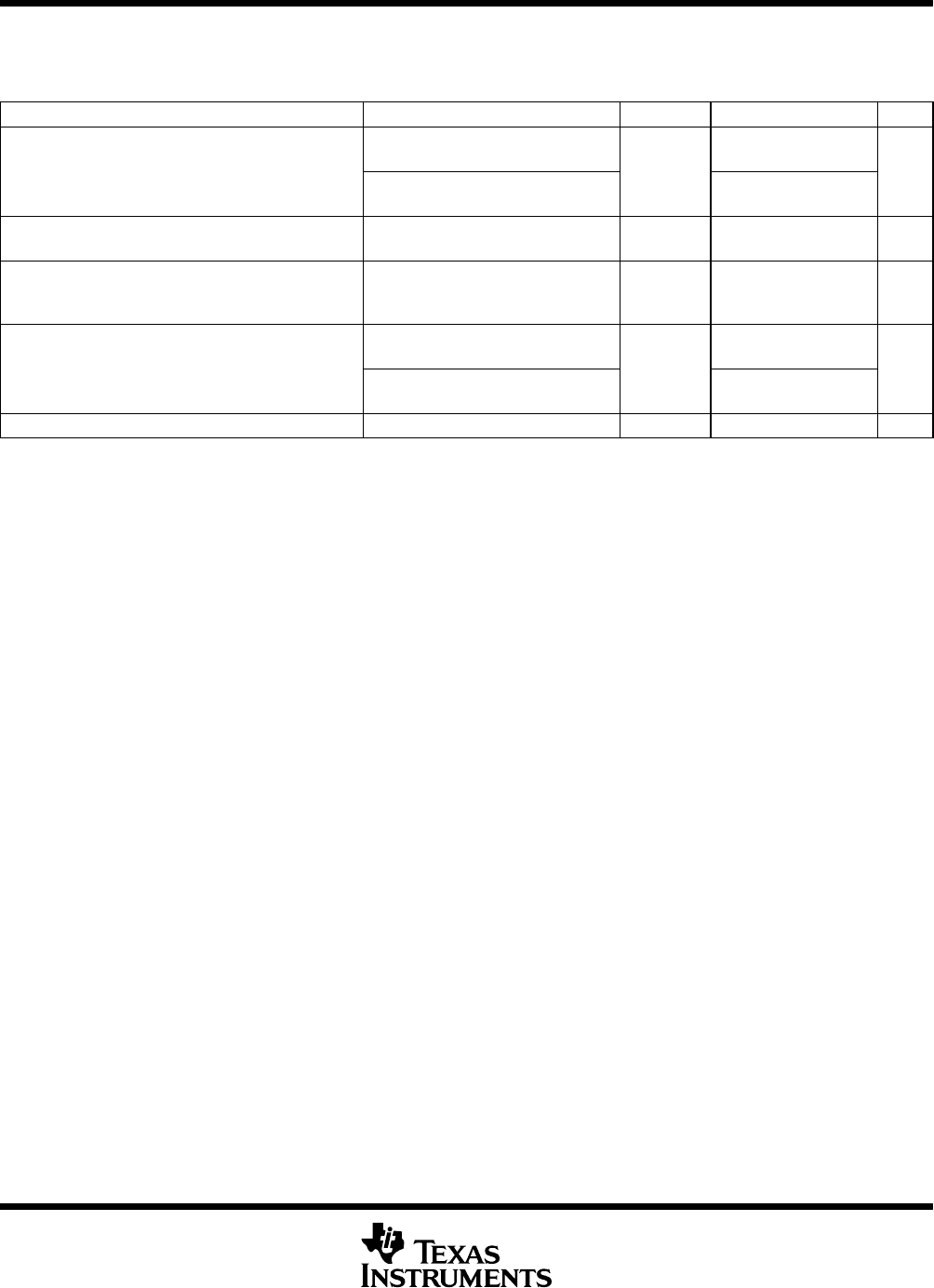
electrical characteristics over recommended ranges of supply voltage and operating free-air
temperature (unless otherwise noted) (continued)
10-bit ADC, external reference (see Note 1)
PARAMETER TEST CONDITIONS VCC MIN TYP MAX UNIT
Positive external reference input
V
eREF+
> V
eREF−
,
SREF1 = 1, SREF0 = 0
1.4 V
CC
V
eREF+
voltage range (see Note 2)
V
eREF−
≤ V
eREF+
≤ V
CC
− 0.15 V,
SREF1 = 1, SREF0 = 1 (see Note 3)
1.4 3.0
V
V
eREF−
Negative external reference input
voltage range (see Note 4)
V
eREF+
> V
eREF−
0 1.2 V
ΔV
eREF
Differential external reference input
voltage range
ΔV
eREF
= V
eREF+
− V
eREF−
V
eREF+
> V
eREF−
(see Note 5) 1.4 V
CC
V
Static input current into V
0V ≤ V
eREF+
≤ V
CC
,
SREF1 = 1, SREF0 = 0
±1
I
VeREF+
Static input current into V
eREF+
0V ≤V
eREF+
≤ V
CC
− 0.15 V ≤ 3 V,
SREF1 = 1, SREF0 = 1 (see Note 3)
2.2 V/3 V
0
μA
I
VeREF−
Static input current into V
eREF−
0V ≤ V
eREF−
≤ V
CC
2.2 V/3 V ±1 μA
NOTES: 1. The external reference is used during conversion to charge and discharge the capacitance array. The input capacitance, C
I
, is also
the dynamic load for an external reference during conversion. The dynamic impedance of the reference supply should follow the
recommendations on analog-source impedance to allow the charge to settle for 10-bit accuracy.
2. The accuracy limits the minimum positive external reference voltage. Lower reference voltage levels may be applied with reduced
accuracy requirements.
3. Under this condition, the external reference is internally buffered. The reference buffer is active and requires the reference buffer
supply current I
REFB
. The current consumption can be limited to the sample and conversion period with REBURST = 1.
4. The accuracy limits the maximum negative external reference voltage. Higher reference voltage levels may be applied with reduced
accuracy requirements.
5. The accuracy limits the minimum external differential reference voltage. Lower differential reference voltage levels may be applied
with reduced accuracy requirements.


