MSP430x22x2, MSP430x22x4
MIXED SIGNAL MICROCONTROLLER
SLAS504B − JULY 2006 − REVISED JULY 2007
42
POST OFFICE BOX 655303 • DALLAS, TEXAS 75265
POST OFFICE BOX 1443 • HOUSTON, TEXAS 77251−1443
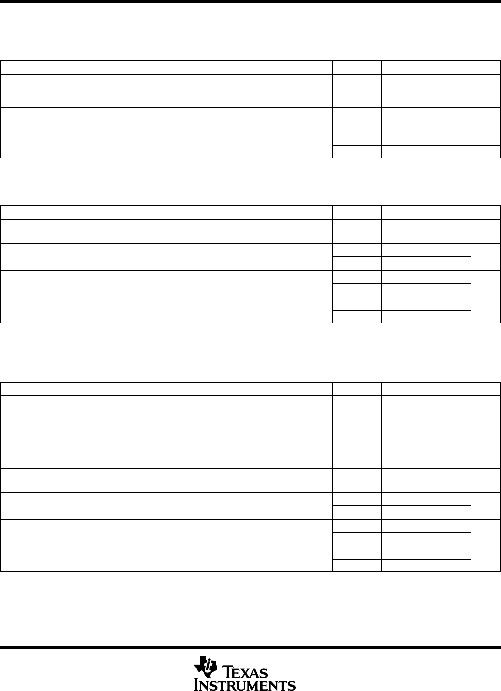
electrical characteristics over recommended ranges of supply voltage and operating free-air
temperature (unless otherwise noted) (continued)
USCI (UART Mode)
PARAMETER TEST CONDITIONS VCC MIN TYP MAX UNIT
f
USCI
USCI input clock frequency
Internal: SMCLK, ACLK
External: UCLK
Duty cycle = 50% ± 10%
f
SYSTEM
MHz
f
BITCLK
BITCLK clock frequency
(equals baud rate in MBaud)
2.2V /3 V 1 MHz
UART receive de
litch time
2.2 V 50 150 600 ns
t
τ
(see Note 1)
3 V 50 100 600 ns
NOTES: 1. Pulses on the UART receive input (UCxRX) shorter than the UART receive deglich time are suppressed. To ensure that pulses are
correctly recognized, their width should exceed the maximum specification of the deglitch time.
USCI (SPI Master Mode, see Figure 20 and Figure 21)
PARAMETER TEST CONDITIONS VCC MIN TYP MAX UNIT
f
USCI
USCI input clock frequency
SMCLK, ACLK
Duty cycle = 50% ± 10%
f
SYSTEM
MHz
SOMI input data setup time
2.2 V 110
t
SU,MI
SOMI input data setup time
3 V 75
ns
SOMI input data hold time
2.2 V 0
t
HD,MI
SOMI input data hold time
3 V 0
ns
SIMO output data valid time
UCLK ed
e to SIMO valid,
2.2 V 30
t
VALID,MO
SIMO output data valid time
,
C
L
= 20 pF
3 V 20
ns
NOTE: f
UCxCLK
+
1
2t
LOńHI
with t
LOńHI
w max(t
VALID,MO(USCI)
) t
SU,SI(Slave),
t
SU,MI(USCI)
) t
VALID,SO(Slave)
).
For the slave’s parameters t
SU,SI(Slave)
and t
VALID,SO(Slave)
, see the SPI parameters of the attached slave.
USCI (SPI Slave Mode, see Figure 22 and Figure 23)
PARAMETER TEST CONDITIONS VCC MIN TYP MAX UNIT
t
STE,LEAD
STE lead time
STE low to clock
2.2 V/3 V 50 ns
t
STE,LAG
STE lag time
Last clock to STE high
2.2 V/3 V 10 ns
t
STE,ACC
STE access time
STE low to SOMI data out
2.2 V/3 V 50 ns
t
STE,DIS
STE disable time
STE high to SOMI high impedance
2.2 V/3 V 50 ns
SIMO input data setup time
2.2 V 20
t
SU,SI
SIMO input data setup time
3 V 15
ns
SIMO input data hold time
2.2 V 10
t
HD,SI
SIMO input data hold time
3 V 10
ns
SOMI output data valid time
UCLK edge to SOMI valid,
2.2 V 75 110
t
VALID,SO
SOMI output data valid time
,
C
L
= 20 pF
3 V 50 75
ns
NOTE: f
UCxCLK
+
1
2t
LOńHI
with t
LOńHI
w max(t
VALID,MO(Master)
) t
SU,SI(USCI),
t
SU,MI(Master)
) t
VALID,SO(USCI)
).
For the master’s parameters t
SU,MI(Master)
and t
VALID,MO(Master)
, see the SPI parameters of the attached master.


