Freelance Electronics Components Distributor
Closed Dec 25th-26th
800-300-1968
We Stock Hard to Find Parts

MAX186ACWP

Part # MAX186ACWP
Description IC DAS 8CH 12BIT T/H LP 20-SOIC
Category IC
Availability In Stock
Qty 72
Qty Price
1 - 15 $17.49752
16 - 30 $13.91849
31 - 45 $13.12314
46 - 60 $12.19524
61 + $10.86967
Manufacturer Available Qty
MAXIM
Date Code: 0627
  • Shipping Freelance Stock: 72
    Ships Immediately


Technical Document


DISCLAIMER: The information provided herein is solely for informational purposes. Customers must be aware of the suitability of this product for their application, and consider that variable factors such as Manufacturer, Product Category, Date Codes, Pictures and Descriptions may differ from available inventory.

Using the buffered REFADJ input avoids external
buffering of the reference. To use the direct VREF input,
disable the internal buffer by tying REFADJ to V
DD
.
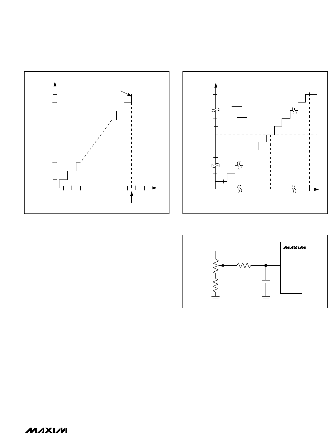
Transfer Function and Gain Adjust
Figure 15 depicts the nominal, unipolar input/output
(I/O) transfer function, and Figure 16 shows the bipolar
input/output transfer function. Code transitions occur
halfway between successive integer LSB values. Output
coding is binary with 1 LSB = 1.00mV (4.096V/4096) for
unipolar operation and 1 LSB = 1.00mV ((4.096V/2 -
-4.096V/2)/4096) for bipolar operation.
Figure 17, the MAX186 Reference-Adjust Circuit, shows
how to adjust the ADC gain in applications that use the
internal reference. The circuit provides ±1.5%
(±65LSBs) of gain adjustment range.
Layout, Grounding, Bypassing
For best performance, use printed circuit boards.
Wire-wrap boards are not recommended. Board layout
should ensure that digital and analog signal lines are
separated from each other. Do not run analog and digi-
tal (especially clock) lines parallel to one another, or
digital lines underneath the ADC package.
Figure 18 shows the recommended system ground
connections. A single-point analog ground (“star”
ground point) should be established at AGND, sepa-
rate from the logic ground. All other analog grounds
and DGND should be connected to this ground. No
other digital system ground should be connected to
this single-point analog ground. The ground return to
the power supply for this ground should be low imped-
ance and as short as possible for noise-free operation.
High-frequency noise in the V
DD
power supply may
affect the high-speed comparator in the ADC. Bypass
these supplies to the single-point analog ground with
0.1µF and 4.7µF bypass capacitors close to the
MAX186/MAX188. Minimize capacitor lead lengths for
best supply-noise rejection. If the +5V power supply is
very noisy, a 10 resistor can be connected as a low-
pass filter, as shown in Figure 18.
MAX186/MAX188
Low-Power, 8-Channel,
Serial 12-Bit ADCs
______________________________________________________________________________________ 19
OUTPUT CODE
FULL-SCALE
TRANSITION
11 . . . 111
11 . . . 110
11 . . . 101
00 . . . 011
00 . . . 010
00 . . . 001
00 . . . 000
123
0
FS
FS - 3/2LSB
FS = +4.096V
1LSB = FS
4096
INPUT VOLTAGE (LSBs)
011 . . . 111
011 . . . 110
000 . . . 010
000 . . . 001
000 . . . 000
111 . . . 111
111 . . . 110
111 . . . 101
100 . . . 001
100 . . . 000
-FS
0V
INPUT VOLTAGE (LSBs)
+FS - 1LSB
FS = +4.096
2
1LSB = +4.096
4096
+5V
510k
100k
24k
0.01µF
12
REFADJ
MAX186
Figure 17. MAX186 Reference-Adjust Circuit
Figure 15. MAX186/MAX188 Unipolar Transfer Function,
4.096V = Full Scale
Figure 16. MAX186/MAX188 Bipolar Transfer Function,
±4.096V/2 = Full Scale
MAX186/MAX188
High-Speed Digital Interfacing with QSPI
The MAX186/MAX188 can interface with QSPI at high
throughput rates using the circuit in Figure 19. This
QSPI circuit can be programmed to do a conversion on
each of the eight channels. The result is stored in mem-
ory without taxing the CPU since QSPI incorporates its
own micro-sequencer. Figure 19 depicts the MAX186,
but the same circuit could be used with the MAX188 by
adding an external reference to VREF and connecting
REFADJ to V
DD
.
Figure 20 details the code that sets up QSPI for
autonomous operation. In external clock mode, the
MAX186/MAX188 perform a single-ended, unipolar con-
version on each of their eight analog input channels.
Figure 21, QSPI Assembly-Code Timing, shows the tim-
ing associated with the assembly code of Figure 20. The
first byte clocked into the MAX186/MAX188 is the control
byte, which triggers the first conversion on CH0. The last
two bytes clocked into the MAX186/MAX188 are all zero
and clock out the results of the CH7 conversion.
Low-Power, 8-Channel,
Serial 12-Bit ADCs
20 ______________________________________________________________________________________
+5V
-5V
GND
SUPPLIES
DGND+5VDGNDV
SS
AGNDV
DD
DIGITAL
CIRCUITRY
MAX186/MAX188
R* = 10
* OPTIONAL
Figure 18. Power-Supply Grounding Connection
20
19
18
17
16
15
14
13
12
11
2
3
4
5
6
7
8
9
10
MAX186
CH0
CH1
CH2
CH3
CH4
CH5
CH6
CH7
V
SS
SHDN
V
DD
SCLK
CS
DIN
SSTRB
DOUT
DGND
AGND
REFADJ
VREF
V
DDI
, V
DDE
, V
DDSYN
, V
STBY
SCK
PCS0
MOSI
MISO
* CLOCK CONNECTIONS NOT SHOWN
V
SSI
VSSE
MC68HC16
0.1µF 4.7µF
0.01µF
0.1µF
4.7µF
ANALOG 
INPUTS
+5V
+
1
Figure 19. MAX186 QSPI Connection
MAX186/MAX188
Low-Power, 8-Channel,
Serial 12-Bit ADCs
______________________________________________________________________________________ 21
*Title : MAX186.ASM
* Description :
* This is a shell program for using a stand-alone 68HC16 without any external memory. The internal 1K RAM
* is put into bank $0F to maintain 68HC11 code compatibility. This program was written with software
* provided in the Motorola 68HC16 Evaluation Kit.
*
* Roger J.A. Chen, Applications Engineer
* MAXIM Integrated Products
* November 20, 1992
*
******************************************************************************************************************************************************
INCLUDE ‘EQUATES.ASM’ ;Equates for common reg addrs
INCLUDE ‘ORG00000.ASM’ ;initialize reset vector
INCLUDE ‘ORG00008.ASM’ ;initialize interrupt vectors
ORG $0200 ;start program after interrupt vectors
INCLUDE ‘INITSYS.ASM’ ;set EK=F,XK=0,YK=0,ZK=0
;set sys clock at 16.78 MHz, COP off
INCLUDE ‘INITRAM.ASM’ ;turn on internal SRAM at $10000
;set stack (SK=1, SP=03FE)
MAIN:
JSR INITQSPI
MAINLOOP:
JSR READ186
WAIT:
LDAA SPSR
ANDA #$80
BEQ WAIT ;wait for QSPI to finish
BRA MAINLOOP
ENDPROGRAM:
INITQSPI:
;This routine sets up the QSPI microsequencer to operate on its own.
;The sequencer will read all eight channels of a MAX186/MAX188 each time
;it is triggered. The A/D converter results will be left in the
;receive data RAM. Each 16 bit receive data RAM location will
;have a leading zero, 12 bits of conversion result and three zeros.
;
;Receive RAM Bits 15 14 13 12 11 10 09 08 07 06 05 04 03 02 01 00
;A/D Result 0 MSB LSB 0 0 0
***** Initialize the QSPI Registers ******
PSHA
PSHB
LDAA #%01111000
STAA QPDR ;idle state for PCS0-3 = high
LDAA #%01111011
STAA QPAR ;assign port D to be QSPI
LDAA #%01111110
STAA QDDR ;only MISO is an input
LDD #$8008
STD SPCR0 ;master mode,16 bits/transfer,
;CPOL=CPHA=0,1MHz Ser Clock
LDD #$0000
STD SPCR1 ;set delay between PCS0 and SCK,
Figure 20. MAX186/MAX188 Assembly-Code Listing
PREVIOUS12345678NEXT