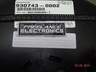
Freelance Electronics Components Distributor
Closed Dec 25th-26th
800-300-1968
We Stock Hard to Find Parts

MAX1820ZEUB

Part # MAX1820ZEUB
Description Switching Voltage RegulatorsWCDMA 600mA Buck Regulator
Category IC
Availability In Stock
Qty 90
Qty Price
1 - 18 $3.38663
19 - 37 $2.69391
38 - 56 $2.53997
57 - 75 $2.36038
76 + $2.10382
Manufacturer Available Qty
MAXIM
  • Shipping Freelance Stock: 90
    Ships Immediately


Technical Document


DISCLAIMER: The information provided herein is solely for informational purposes. Customers must be aware of the suitability of this product for their application, and consider that variable factors such as Manufacturer, Product Category, Date Codes, Pictures and Descriptions may differ from available inventory.

MAX1820ZEUB
Rev. B
RELIABILITY REPORT
FOR
MAX1820ZEUB
PLASTIC ENCAPSULATED DEVICES
March 21, 2003
MAXIM INTEGRATED PRODUCTS
120 SAN GABRIEL DR.
SUNNYVALE, CA 94086
Written by Reviewed by
Jim Pedicord Bryan J. Preeshl
Quality Assurance Quality Assurance
Reliability Lab Manager Executive Director
Conclusion
The MAX1820 successfully meets the quality and reliability standards required of all Maxim products. In addition,
Maxim’s continuous reliability monitoring program ensures that all outgoing product will continue to meet Maxim’s quality
and reliability standards.
Table of Contents
I. ........Device Description V. ........Quality Assurance Information
II. ........Manufacturing Information VI. .......Reliability Evaluation
III. .......Packaging Information
IV. .......Die Information ......Attachments
I. Device Description
A. General
The MAX1820 low-dropout, pulse-width-modulated (PWM) DC-DC buck regulator is optimized to provide power to the
power amplifier (PA) in WCDMA cell phones; however, it may be applied in many other applications where high
efficiency is a priority. The supply voltage range is from 2.6V to 5.5V, and the guaranteed output current is 600mA;
1MHz PWM switching allows for small external components, while skip mode reduces quiescent current to 180µA
with light loads.
The MAX1820 is dynamically controlled to provide varying output voltages from 0.4V to 3.4V. The circuit is designed
such that the output voltage settles in <30µs for a full-scale change in voltage and current.
The MAX1820 includes a low on-resistance internal MOSFET switch and synchronous rectifier to maximize
efficiency and minimize external component count; 100% duty-cycle operation allows for low dropout of only 150mV
at 600mA load, including the external inductor resistance. The device is offered in 10-pin µMAX and tiny 3 x 4 chip-
scale (UCSP™) packages
B. Absolute Maximum Ratings
Item Rating
BATT, OUT (FB), SHDN, SYNC, SKIP, REF to GND -0.3V to +6.0V
PGND to GND -0.3V to +0.3V
LX, COMP to GND -0.3V to (VBATT + 0.3V)
Output Short-Circuit Duration Infinite
Operating Temperature Range -40°C to +85°C
Junction Temperature +150°C
Storage Temperature Ranges -65°C to +150°C
Lead Temperature (soldering, 10s) +300°C
Continuous Power Dissipation (TA = +70°C)
10-Pin µMAX 444mW
Derates above +70°C
10-Pin µMAX 5.6mW/°C
II. Manufacturing Information
A. Description/Function: WCDMA Cellular Phone 600Ma Buck Regulator
B. Process: S8 - Standard 8 micron silicon gate CMOS
C. Number of Device Transistors: 2722
D. Fabrication Location: California, USA
E. Assembly Location: Thailand, Philippines or Malaysia
F. Date of Initial Production: April, 2001
III. Packaging Information
A. Package Type: 10-Lead µMAX
B. Lead Frame: Copper
C. Lead Finish: Solder Plate
D. Die Attach: Silver-filled Epoxy
E. Bondwire: Gold (1.3 mil dia.)
F. Mold Material: Epoxy with silica filler
G. Assembly Diagram: Buildsheet # 05-2301-0048
H. Flammability Rating: Class UL94-V0
I. Classification of Moisture Sensitivity
per JEDEC standard JESD22-A112: Level 1
IV. Die Information
A. Dimensions: 81 X 81 mils
B. Passivation: Si
3
N
4
/SiO
2
(Silicon nitride/ Silicon dioxide)
C. Interconnect: TiW/ AlCu/ TiWN
D. Backside Metallization: None
E. Minimum Metal Width: .8 microns (as drawn)
F. Minimum Metal Spacing: .8 microns (as drawn)
G. Bondpad Dimensions: 2.7 mil. Sq.
H. Isolation Dielectric: SiO
2
I. Die Separation Method: Wafer Saw
123NEXT