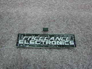
Freelance Electronics Components Distributor
Closed Dec 25th-26th
800-300-1968
We Stock Hard to Find Parts

MAX1778EUG

Part # MAX1778EUG
Description QUAD-OUTPUT TFT LCD DC-DC CONVERTER WITH BUFF - Bulk
Category IC
Availability In Stock
Qty 14
Qty Price
1 - 2 $10.83507
3 - 5 $8.61881
6 - 8 $8.12631
9 - 11 $7.55172
12 + $6.73088
Manufacturer Available Qty
MAXIM
Date Code: 0100
  • Shipping Freelance Stock: 14
    Ships Immediately


Technical Document


DISCLAIMER: The information provided herein is solely for informational purposes. Customers must be aware of the suitability of this product for their application, and consider that variable factors such as Manufacturer, Product Category, Date Codes, Pictures and Descriptions may differ from available inventory.

General Description
The MAX1778/MAX1880–MAX1885 multiple-output
DC-DC converters provide the regulated voltages
required by active matrix thin-film transistor (TFT) liquid
crystal displays (LCD) in a low-profile TSSOP package.
One high-power step-up converter and two low-power
charge pumps convert the 2.7V to 5.5V input voltage
into three independent output voltages. A built-in linear
regulator and VCOM buffer complete the power-supply
requirements.
The main step-up converter accurately generates an
externally set output voltage up to 13V that can supply
the display’s row/column drivers. The converter’s high
switching frequency and current-mode PWM architec-
ture provide fast transient response and allow the use
of small low-profile inductors and ceramic capacitors.
The low-power BiCMOS control circuitry and internal
14V switch (0.35 N-channel MOSFET) enable efficien-
cies up to 91%.
The dual low-power charge pumps (MAX1778/
MAX1880/MAX1881/MAX1882 only) independently reg-
ulate one positive output (V
POS
) and one negative out-
put (V
NEG
). These low-power outputs use external
diode and capacitor stages (as many stages as
required) to regulate output voltages up to +40V and
-40V. A unique control scheme minimizes output ripple
as well as capacitor sizes for both charge pumps.
A resistor-programmable, 40mA, low-dropout linear
regulator (MAX1778/MAX1881/MAX1883/MAX1884
only) provides preregulation or postregulation for any of
the supplies. For higher current applications, an exter-
nal transistor can be added. Additionally, the VCOM
buffer provides a high current output that is ideal for
driving the capacitive backplane of TFT LCD panels.
The VCOM buffer’s output voltage is preset with an
internal 50% resistive-divider or can be externally
adjusted for other voltages.
The MAX1778/MAX1880–MAX1885 are protected
against output undervoltage and thermal overload con-
ditions by a latched fault detection circuit that shuts
down the device. All devices are available in the ultra-
thin TSSOP package (1.1mm max height).
Applications
TFT LCD Notebook Displays
TFT LCD Desktop Monitor Panels
Features
500kHz/1MHz Current-Mode PWM Step-Up
Regulator
Up to +13V Main High-Power Output
±1% Accurate
High Efficiency (91%)
Dual Regulated Charge-Pump Outputs
(MAX1778/MAX1880/MAX1881/MAX1882 only)
Up to +40V Positive Charge-Pump Output
Up to -40V Negative Charge-Pump Output
Low-Dropout 40mA Linear Regulator
(MAX1778/MAX1881/MAX1883/MAX1884 only)
Up to +15V LDO Input
Optional Higher Current with External Transistor
2.7V to 5.5V Input Supply
Internal Supply Sequencing and Soft-Start
Power-Ready Output
Adjustable Fault-Detection Latch
Thermal Protection (+160°C)
0.1µA Shutdown Current
0.7mA IN Quiescent Current
Ultra-Small External Components
Thin TSSOP Package (1.1mm max height)
MAX1778/MAX1880–MAX1885
Quad-Output TFT LCD DC-DC
Converters with Buffer
________________________________________________________________ Maxim Integrated Products 1
19-1979; Rev 0a; 3/01
Ordering Information
PART TEMP. RANGE PIN-PACKAGE
MAX1778EUG -40°C to +85°C 24 TSSOP
MAX1880EUG -40°C to +85°C 24 TSSOP
MAX1881EUG -40°C to +85°C 24 TSSOP
MAX1882EUG -40°C to +85°C 24 TSSOP
MAX1883EUP -40°C to +85°C 20 TSSOP
MAX1884EUP -40°C to +85°C 20 TSSOP
MAX1885EUP -40°C to +85°C 20 TSSOP
Typical Operating Circuit appears at end of data sheet.
Pin Configurations and Selector Guide appear at end of
data sheet.
For pricing, delivery, and ordering information, please contact Maxim/Dallas Direct! at
1-888-629-4642, or visit Maxim’s website at www.maxim-ic.com.
MAX1778/MAX1880–MAX1885
Quad-Output TFT LCD DC-DC
Converters with Buffer
2 _______________________________________________________________________________________
ABSOLUTE MAXIMUM RATINGS
ELECTRICAL CHARACTERISTICS
(V
IN
= +3.0V, SHDN = IN, V
SUPP
= V
SUPN
= V
SUPB
= V
SUPL
= 10V, LDOOUT = FBL, BUF- = BUFOUT, BUF+ = FLTSET = TGND =
PGND = GND, C
REF
= 0.22µF, C
BUF
= 1µF, T
A
= 0°C to +85°C. Typical values are at T
A
= +25°C, unless otherwise noted.)
Stresses beyond those listed under “Absolute Maximum Ratings” may cause permanent damage to the device. These are stress ratings only, and functional
operation of the device at these or any other conditions beyond those indicated in the operational sections of the specifications is not implied. Exposure to
absolute maximum rating conditions for extended periods may affect device reliability.
IN, SHDN, TGND, FLTSET to GND...........................-0.3V to +6V
DRVN to GND .........................................-0.3V to (V
SUPN
+ 0.3V)
DRVP to GND..........................................-0.3V to (V
SUPP
+ 0.3V)
PGND to GND.....................................................................±0.3V
RDY, SUPB to GND ................................................-0.3V to +14V
LX, SUPP, SUPN to PGND .....................................-0.3V to +14V
SUPL to GND..........................................................-0.3V to +18V
LDOOUT to GND ....................................-0.3V to (V
SUPL
+ 0.3V)
INTG, REF, FB, FBN, FBP to GND...............-0.3V to (V
IN
+ 0.3V)
FBL to GND .............-0.3V to the lower of (V
SUP
L
+ 0.3V) or +6V
BUFOUT, BUF+, BUF- to GND ...............-0.3V to (V
SUPB
+ 0.3V)
Continuous Power Dissipation (T
A
= +70°C)
20-Pin TSSOP (derate 10.9mW/°C above +70°C) ......879mW
24-Pin TSSOP (derate 12.2mW/°C above +70°C) ......975mW
Operating Temperature Range
MAX1778EUG, MAX1883EUP ........................-40°C to +85°C
Junction Temperature......................................................+150°C
Storage Temperature Range .............................-65°C to +150°C
Lead Temperature (soldering, 10s) .................................+300°C
PARAMETER SYMBOL CONDITIONS MIN TYP MAX UNITS
Input Supply Range V
IN
2.7 5.5 V
Input Undervoltage Threshold V
UVLO
V
IN
rising, 40mV hysteresis (typ) 2.2 2.4 2.6 V
MAX1778/MAX1880/
MAX1883 (f
OSC
= 1MHz)
0.7 1
IN Quiescent Supply Current I
IN
V
FB
= V
FBP
= 1.5V, V
FBN
= -0.2V
MAX1881/MAX1882/
MAX1884/MAX1885
(f
OSC
= 500kHz)
0.6 1
mA
MAX1778/MAX1880
(f
OSC
= 1MHz)
0.4 0.7
SUPP Quiescent Current I
SUPP
V
FBP
= 1.5V
MAX1881/MAX1882
(f
OSC
= 500kHz)
0.3 0.5
mA
MAX1778/MAX1880
(f
OSC
= 1MHz)
0.4 0.7
SUPN Quiescent Current I
SUPN
V
FBN
= -0.2V
MAX1881/MAX1882
(f
OSC
= 500kHz)
0.3 0.5
mA
IN Shutdown Current V
SHDN
= 0, V
IN
= 5V 0.1 10 µA
SUPP Shutdown Current
V
SHDN
= 0, V
SUPP
= 13V,
MAX1778/MAX1880/MAX1881/MAX1882
0.1 10 µA
SUPN Shutdown Current
V
SHDN
= 0, V
SUPN
= 13V,
MAX1778/MAX1880/MAX1881/MAX1882
0.1 10 µA
SUPL Shutdown Current
V
SHDN
= 0, V
SUPL
= 13V
MAX1778/MAX1881/MAX1883/MAX1884
0.1 10 µA
SUPB Shutdown Current V
SHDN
= 0, V
SUPB
= 13V 6 13 µA
MAX1778/MAX1880–MAX1885
Quad-Output TFT LCD DC-DC
Converters with Buffer
_______________________________________________________________________________________ 3
ELECTRICAL CHARACTERISTICS (continued)
(V
IN
= +3.0V, SHDN = IN, V
SUPP
= V
SUPN
= V
SUPB
= V
SUPL
= 10V, LDOOUT = FBL, BUF- = BUFOUT, BUF+ = FLTSET = TGND =
PGND = GND, C
REF
= 0.22µF, C
BUF
= 1µF, T
A
= 0°C to +85°C. Typical values are at T
A
= +25°C, unless otherwise noted.)
PARAMETER SYMBOL
CONDITIONS MIN TYP MAX
UNITS
MAIN STEP-UP CONVERTER
Main Output Voltage Range V
MAIN
V
IN
13
V
Integrator enabled, C
INTG
= 1000pF 1.234 1.247 1.260
FB Regulation Voltage V
FB
Integrator disabled (INTG = REF) 1.220 1.280
V
FB Input Bias Current I
FB
V
FB
= 1.25V, INTG = GND -50 +50
nA
MAX1778/MAX1880/MAX1883 0.85 1 1.15
MHz
Operating Frequency f
OSC
MAX1881/MAX1882/MAX1884/MAX1885 425 500 575
kHz
Oscillator Maximum Duty
Cycle
80 85 91 %
Integrator enabled,
C
INTG
= 1000pF
0.01
Load Regulation
I
LX
= 0 to 200mA,
V
MAIN
= 10V
Integrator disabled
(INTG = REF)
0.2
%
Line Regulation 0.1 %/V
Integrator Transconductance 317 µs
LX Switch On-Resistance R
LX
(
ON
)
I
LX
= 100mA 0.35 0.7
LX Leakage Current I
LX
V
LX
= 13V 0.01 20 µA
Phase I = soft-start (1024/f
OSC
) 0.275 0.38 0.5
Phase II = soft-start (1024/f
OSC
) 0.75
Phase III = soft-start (1024/f
OSC
) 1.12
LX Current Limit I
LIM
Phase IV = fully-on (after 3072/f
OSC
) 1.15 1.5 1.85
A
Maximum RMS LX Current 1A
Soft-Start Period t
SS
Power-up to the end of Phase III 3072 / f
OSC
s
Falling edge, FLTSET = GND 1.07 1.1 1.14
FB Fault Trip Level
Falling edge, FLTSET = 1V 0.955 0.99 1.025
V
POSITIVE CHARGE PUMP (MAX1778/MAX1880/MAX1881/MAX1882 ONLY)
SUPP Input Supply Range
V
SUPP
2.7 13 V
Operating Frequency f
CHP
0.5 x f
OSC
Hz
FBP Regulation Voltage V
FBP
1.2 1.25 1.3
V
FBP Input Bias Current I
FBP
V
FBP
= 1.5V -50 +50
nA
DRVP PCH On-Resistance R
PCH
(
ON
)
510
V
FBP
= 1.2V 2 4
DRVP NCH On-Resistance R
NCH
(
ON
)
V
FBP
= 1.3V 20
k
Maximum RMS DRVP Current 0.1
A
FBP Power-Ready Trip Level Rising edge 1.09 1.125 1.16
V
Falling edge, FLTSET = GND 1.08 1.11 1.16
FBP Fault Trip Level
Falling edge, FLTSET = 1V 0.955 0.99 1.025
V
1234567NEXT