Closed Dec 25th-26th
800-300-1968
We Stock Hard to Find Parts
My Account
|
My Orders
|
My Cart
Questions?
(800) 300-1968
Register
(current)
My Account
(current)
My Orders
(current)
My Cart
(current)
Categories
(current)
Manufacturers
Request a Quote
Sell Your Excess
Consignment
Quality Assurance
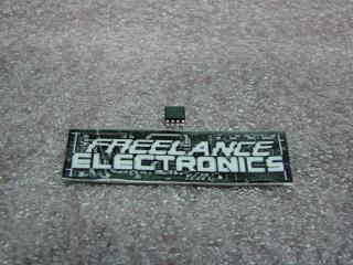
MAX1711EEG
Part #
MAX1711EEG
Description
IC CTRLR HS 4-BIT ADJ 24-QSOP
Category
IC
Availability
In Stock
Qty
14
Qty
Price
1 - 2
$3.43191
3 - 5
$2.72993
6 - 8
$2.57393
9 - 11
$2.39194
12 +
$2.13194
Manufacturer
Available
Qty
MAXIM
Date Code: 0000
Freelance Stock:
14
Ships Immediately
Add to Cart
Related Items
MAXIM
IC
MAX1709ESE
$4.91297
MAXIM
IC
MAX1712EEG
$4.60248
MAXIM
IC
MAX1717EEG
$6.93112
MAXIM
IC
MAX1771CSA
$1.42580
MAXIM
IC
MAX1771CSA+
$4.77602
MAXIM
IC
MAX1776EUA+
$8.43112