Freelance Electronics Components Distributor
Closed Dec 25th-26th
800-300-1968
We Stock Hard to Find Parts

LM6132BIN

Part # LM6132BIN
Description IC OPAMP GP 11MHZ RRO 8DIP
Category IC
Availability Out of Stock
Qty 0
Qty Price
1 + $1.62390


Technical Document


DISCLAIMER: The information provided herein is solely for informational purposes. Customers must be aware of the suitability of this product for their application, and consider that variable factors such as Manufacturer, Product Category, Date Codes, Pictures and Descriptions may differ from available inventory.

Typical Performance Characteristics T
A
= 25˚C, R
L
=10kunless otherwise specified (Continued)
dV
OS
vs
Output Voltage
DS012349-16
dV
OS
vs
Output Voltage
DS012349-17
CMRR vs Frequency
DS012349-18
Output Voltage vs
Sinking Current
DS012349-19
Output Voltage vs
Sinking Current
DS012349-20
Output Voltage vs
Sinking Current
DS012349-21
Output Voltage vs
Sourcing Current
DS012349-22
Output Voltage vs
Sourcing Current
DS012349-23
Output Voltage vs
Sourcing Current
DS012349-24
LM6132/LM6134
www.national.com7
Typical Performance Characteristics T
A
= 25˚C, R
L
=10kunless otherwise specified (Continued)
LM6132/34 Application Hints
The LM6132 brings a new level of ease of use to opamp sys-
tem design.
With greater than rail-to-rail input voltage range concern
over exceeding the common-mode voltage range is elimi-
nated.
Rail-to-rail output swing provides the maximum possible dy-
namic range at the output. This is particularly important
when operating on low supply voltages.
The high gain-bandwidth with low supply current opens new
battery powered applications, where high power consump-
tion, previously reduced battery life to unacceptable levels.
To take advantage of these features, some ideas should be
kept in mind.
ENHANCED SLEW RATE
Unlike most bipolar opamps, the unique phase reversal
prevention/speed-up circuit in the input stage eliminates
phase reversal and allows the slew rate to be very much a
function of the input signal amplitude.
Figure 2
shows how excess input signal is routed around the
input collector-base junctions directly to the current mirrors.
The LM6132/34 input stage converts the input voltage
change to a current change. This current change drives the
current mirrors through the collectors of Q1Q2, Q3Q4
when the input levels are normal.
Noise Voltage vs
Frequency
DS012349-25
Noise Current vs
Frequency
DS012349-38
NF vs Source Resistance
DS012349-39
Gain and Phase vs
Frequency
DS012349-28
Gain and Phase vs
Frequency
DS012349-29
Gain and Phase vs
Frequency
DS012349-30
GBW vs Supply
Voltage at 20 kHz
DS012349-31
LM6132/LM6134
www.national.com 8
LM6132/34 Application Hints
(Continued)
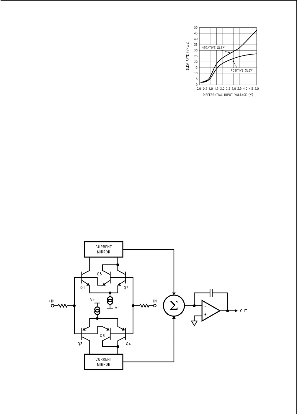
If the input signal exceeds the slew rate of the input stage
and the differential input voltage rises above a diode drop,
the excess signal bypasses the normal input transistors,
(Q1–Q4), and is routed in correct phase through the two ad-
ditional transistors, (Q5, Q6), directly into the current mirrors.
This rerouting of excess signal allows the slew-rate to in-
crease by a factor of 10 to 1 or more. (See
Figure 1
.)
As the overdrive increases, the opamp reacts better than a
conventional opamp. Large fast pulses will raise the slew-
rate to around 25V to 30V/µs.
This effect is most noticeable at higher supply voltages and
lower gains where incoming signals are likely to be large.
This speed-up action adds stability to the system when driv-
ing large capacitive loads.
DRIVING CAPACITIVE LOADS
Capacitive loads decrease the phase margin of all opamps.
This is caused by the output resistance of the amplifier and
the load capacitance forming an R-C phase lag network.
This can lead to overshoot, ringing and oscillation. Slew rate
limiting can also cause additional lag. Most opamps with a
fixed maximum slew-rate will lag further and further behind
when driving capacitive loads even though the differential in-
put voltage raises. With the LM6132, the lag causes the slew
rate to raise. The increased slew-rate keeps the output fol-
lowing the input much better. This effectively reduces phase
lag. After the output has caught up with the input, the differ-
ential input voltage drops down and the amplifier settles
rapidly.
These features allow the LM6132 to drive capacitive loads
as large as 500 pF at unity gain and not oscillate. The scope
photos (
Figure 3
and
Figure 4
) above show the LM6132 driv-
ing a 500 pF load. In
Figure 3
, the lower trace is with no ca-
pacitive load and the upper trace is with a 500 pF load. Here
we are operating on
±
12V supplies with a 20 Vp-p pulse. Ex-
Slew Rate vs Differential V
IN
V
S
=
±
12V
DS012349-40
FIGURE 1.
DS012349-36
FIGURE 2.
LM6132/LM6134
www.national.com9
PREVIOUS12345NEXT