Closed Dec 25th-26th
800-300-1968
We Stock Hard to Find Parts
My Account
|
My Orders
|
My Cart
Questions?
(800) 300-1968
Register
(current)
My Account
(current)
My Orders
(current)
My Cart
(current)
Categories
(current)
Manufacturers
Request a Quote
Sell Your Excess
Consignment
Quality Assurance
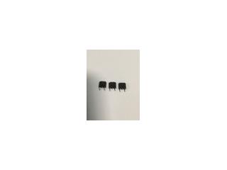
IRFR120
Part #
IRFR120
Description
MOSFET N-CH 100V 7.7A DPAK
Category
IC
Availability
In Stock
Qty
505
Qty
Price
1 - 106
$0.43396
107 - 212
$0.34520
213 - 318
$0.32547
319 - 424
$0.30246
425 +
$0.26958
Manufacturer
Available
Qty
Freelance Stock:
19
Ships Immediately
International Rectifier
Date Code: 0000
Freelance Stock:
486
Ships Immediately
Add to Cart
Related Items
International Rectifier
IC
IRFR12N25DPBF
$2.47511
International Rectifier
RECTIFIER
IRFR1205
$1.26567
Fairchild Semiconductor
IC
008-25424
$11.58351
Harris Corporation
IC
01-6945-9
Motorola Corp
IC
010-143121-0002
Texas Instruments
IC
01295-672141D