Closed Dec 25th-26th
800-300-1968
We Stock Hard to Find Parts
My Account
|
My Orders
|
My Cart
Questions?
(800) 300-1968
Register
(current)
My Account
(current)
My Orders
(current)
My Cart
(current)
Categories
(current)
Manufacturers
Request a Quote
Sell Your Excess
Consignment
Quality Assurance
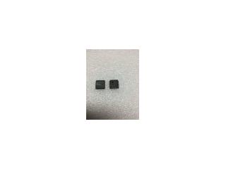
GAL26CV12B-20LJ
Part #
GAL26CV12B-20LJ
Description
IC CPLD 12MC 20NS 28PLCC
Category
IC
Availability
Out of Stock
Qty
0
Qty
Price
1 +
$8.79584
Related Items
Generic
IC
GAL26CLV12D-5LJ
$4.22710
Generic
IC
GAL26CV12-20LJ
Generic
IC
GAL26CV12B-15LJI
$4.47183
Generic
IC
GAL26CV12B-15LP
$9.74069
Generic
IC
GAL26CV12B10LP
$2.44686
Fairchild Semiconductor
IC
008-25424
$11.58351