Closed Dec 25th-26th
800-300-1968
We Stock Hard to Find Parts
My Account
|
My Orders
|
My Cart
Questions?
(800) 300-1968
Register
(current)
My Account
(current)
My Orders
(current)
My Cart
(current)
Categories
(current)
Manufacturers
Request a Quote
Sell Your Excess
Consignment
Quality Assurance
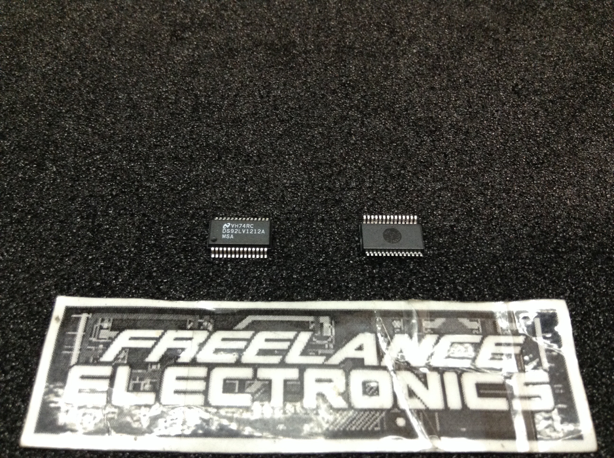
DS92LV1212AMSA
Part #
DS92LV1212AMSA
Description
IC DESERIALIZER 10-BIT 28-SSOP
Category
IC
Availability
Out of Stock
Qty
0
Qty
Price
1 +
$9.46970
Related Items
National Semiconductor Corp
IC
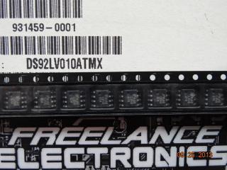
DS92LV010ATMX
$2.03467
National Semiconductor Corp
IC
DS92LV1021AMSA
$10.53273
National Semiconductor Corp
IC
DS92LV1021TMSA
$9.81204
National Semiconductor Corp
IC
DS92LV1210TMSA
$15.09370
Fairchild Semiconductor
IC
008-25424
$11.58351
Harris Corporation
IC
01-6945-9