Closed Dec 25th-26th
800-300-1968
We Stock Hard to Find Parts
My Account
|
My Orders
|
My Cart
Questions?
(800) 300-1968
Register
(current)
My Account
(current)
My Orders
(current)
My Cart
(current)
Categories
(current)
Manufacturers
Request a Quote
Sell Your Excess
Consignment
Quality Assurance
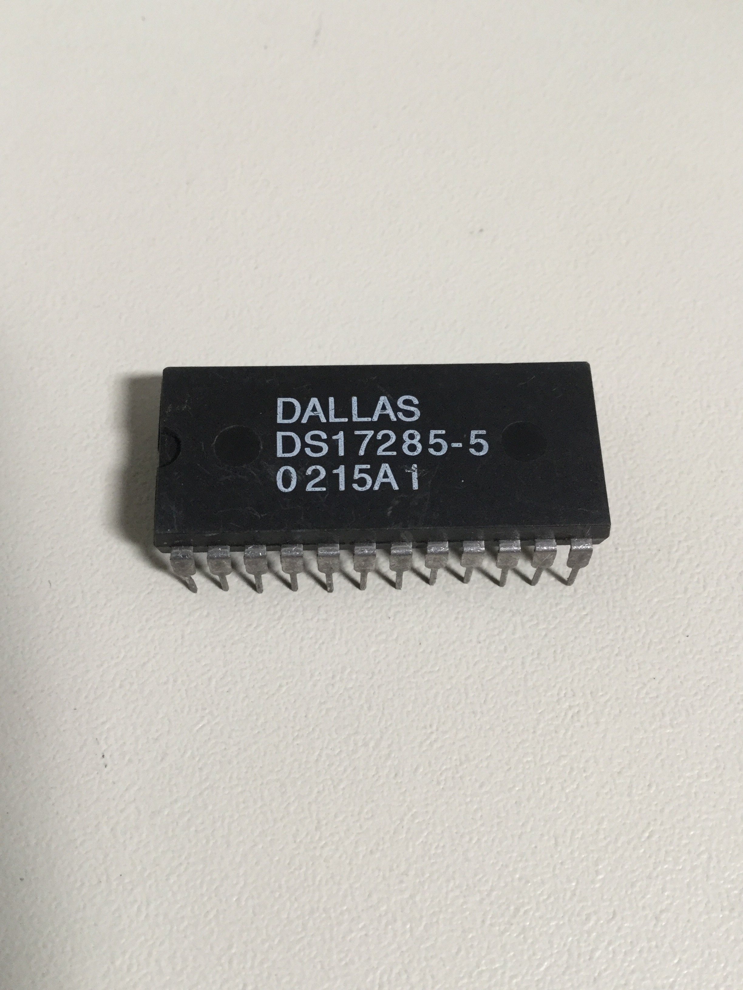
DS17285-5
Part #
DS17285-5
Description
IC RTC CLK/CALENDAR PAR 24-DIP
Category
IC
Availability
In Stock
Qty
3
Qty
Price
1 +
$6.46076
Manufacturer
Available
Qty
DALLAS SEMICONDUCTOR
Date Code: 0200
Freelance Stock:
3
Ships Immediately
Add to Cart
Related Items
Military Spec
IC
DS1720
$7.23245
MAXIM
IC
DS1721S+T&R
$4.83376
MAXIM
IC
DS1726U
$2.53330
Fairchild Semiconductor
IC
008-25424
$11.58351
Harris Corporation
IC
01-6945-9
Motorola Corp
IC
010-143121-0002