CY7C027/028
CY7C037/038
Document #: 38-06042 Rev. *A Page 7 of 19
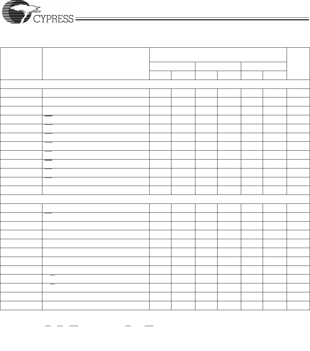
Switching Characteristics Over the Operating Range
[14]
Parameter Description
CY7C027/028
CY7C037/038
Unit
-12
[1]
-15 -20
Min. Max. Min. Max. Min. Max.
READ CYCLE
t
RC
Read Cycle Time 12 15 20 ns
t
AA
Address to Data Valid 12 15 20 ns
t
OHA
Output Hold From Address Change 3 3 3 ns
t
ACE
[15]
CE LOW to Data Valid 12 15 20 ns
t
DOE
OE LOW to Data Valid 8 10 12 ns
t
LZOE
[16, 17, 18]
OE LOW to Low Z 3 3 3 ns
t
HZOE
[16, 17, 18]
OE HIGH to High Z 10 10 12 ns
t
LZCE
[16, 17, 18]
CE LOW to Low Z 3 3 3 ns
t
HZCE
[16, 17, 18]
CE HIGH to High Z 10 10 12 ns
t
PU
[18]
CE LOW to Power-Up 0 0 0 ns
t
PD
[18]
CE HIGH to Power-Down 12 15 20 ns
t
ABE
[15]
Byte Enable Access Time 12 15 20 ns
WRITE CYCLE
t
WC
Write Cycle Time 12 15 20 ns
t
SCE
[15]
CE LOW to Write End 10 12 15 ns
t
AW
Address Valid to Write End 10 12 15 ns
t
HA
Address Hold From Write End 0 0 0 ns
t
SA
[15]
Address Set-Up to Write Start 0 0 0 ns
t
PWE
Write Pulse Width 10 12 15 ns
t
SD
Data Set-Up to Write End 10 10 15 ns
t
HD
Data Hold From Write End 0 0 0 ns
t
HZWE
[17, 18]
R/W LOW to High Z 10 10 12 ns
t
LZWE
[17, 18]
R/W HIGH to Low Z 3 3 3 ns
t
WDD
[19]
Write Pulse to Data Delay 25 30 45 ns
t
DDD
[19]
Write Data Valid to Read Data Valid 20 25 30 ns
Notes:
14. Test conditions assume signal transition time of 3 ns or less, timing reference levels of 1.5V, input pulse levels of 0 to 3.0V, and output loading of the specified
I
OI
/I
OH
and 30-pF load capacitance.
15. To access RAM, CE
=L, UB=L, SEM=H. To access semaphore, CE=H and SEM=L. Either condition must be valid for the entire t
SCE
time.
16. At any given temperature and voltage condition for any given device, t
HZCE
is less than t
LZCE
and t
HZOE
is less than t
LZOE
.
17. Test conditions used are Load 2.
18. This parameter is guaranteed by design, but it is not production tested.
19. For information on port-to-port delay through RAM cells from writing port to reading port, refer to Read Timing with Busy waveform.


