Freelance Electronics Components Distributor
Closed Dec 25th-26th
800-300-1968
We Stock Hard to Find Parts

CY7C028-20AC

Part # CY7C028-20AC
Description SRAM Chip Async Dual 5V 1M-bit 64K x 16 20ns 100-Pin TQFP
Category IC
Availability In Stock
Qty 7
Qty Price
1 - 1 $145.06576
2 - 2 $115.39322
3 - 4 $108.79932
5 - 5 $101.10644
6 + $90.11661
Manufacturer Available Qty
CYPRESS SEMICONDUCTOR
Date Code: 0014
  • Shipping Freelance Stock: 7
    Ships Immediately


Technical Document


DISCLAIMER: The information provided herein is solely for informational purposes. Customers must be aware of the suitability of this product for their application, and consider that variable factors such as Manufacturer, Product Category, Date Codes, Pictures and Descriptions may differ from available inventory.

CY7C027/028
CY7C037/038
Document #: 38-06042 Rev. *A Page 4 of 19
Maximum Ratings
[8]
(Above which the useful life may be impaired. For user guide-
lines, not tested.)
Storage Temperature .................................65
°C to +150°C
Ambient Temperature with
Power Applied.............................................55
°C to +125°C
Supply Voltage to Ground Potential............... 0.3V to +7.0V
DC Voltage Applied to Outputs
in High Z State ............................................ 0.5V to +7.0DC
Input Voltage
[9]
...............................................0.5V to +7.0V
Output Current into Outputs (LOW)............................. 20 mA
Static Discharge Voltage........................................... >1100V
Latch-Up Current.................................................... >200 mA
Note:
8. The Voltage on any input or I/O pin cannot exceed the power pin during power-up.
9. Pulse width < 20 ns.
10. Industrial parts are available in CY7C028 and CY7C038 only.
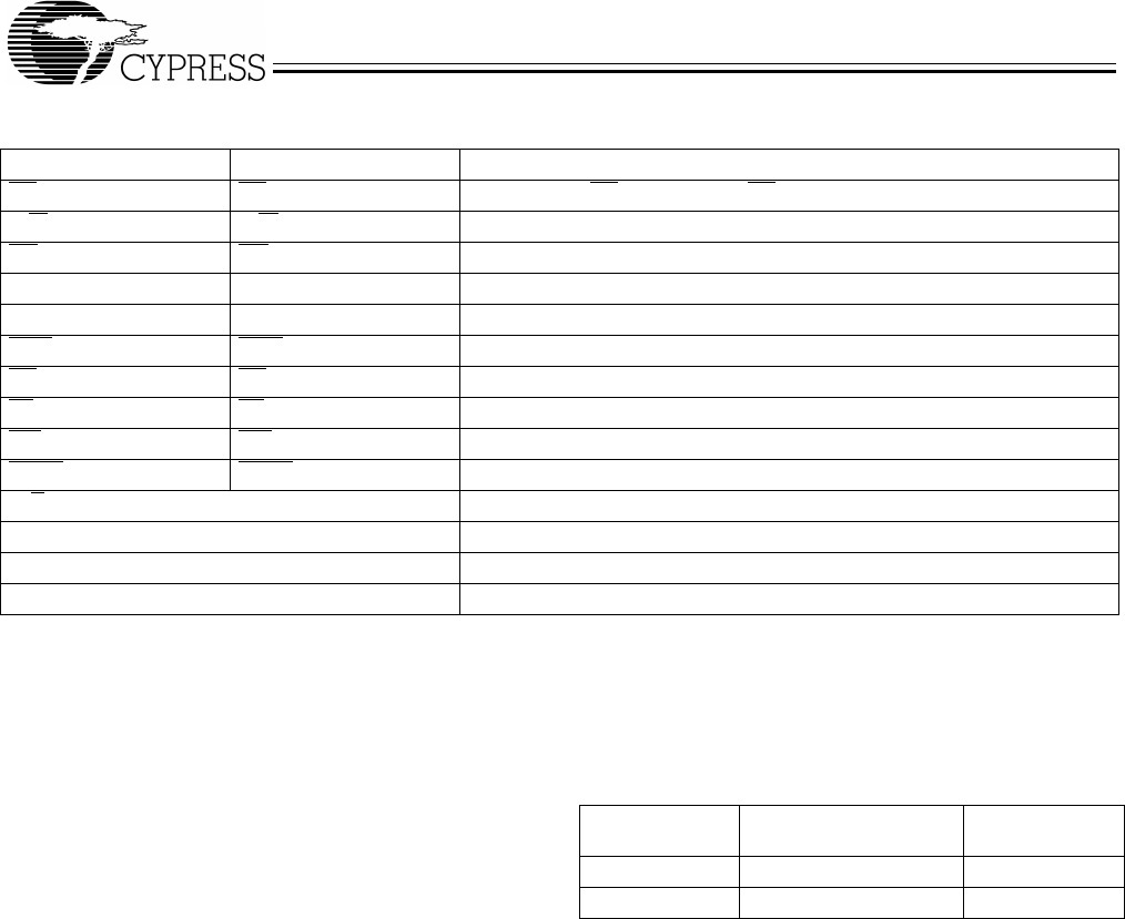
Pin Definitions
Left Port Right Port Description
CE
0L
, CE
1L
CE
0R
, CE
1R
Chip Enable (CE is LOW when CE
0
V
IL
and CE
1
V
IH
)
R/W
L
R/W
R
Read/Write Enable
OE
L
OE
R
Output Enable
A
0L
A
15L
A
0R
A
15R
Address (A
0
A
14
for 32K; A
0
A
15
for 64K devices)
I/O
0L
I/O
17L
I/O
0R
I/O
17R
Data Bus Input/Output (I/O
0
I/O
15
for x16 devices; I/O
0
I/O
17
for x18)
SEM
L
SEM
R
Semaphore Enable
UB
L
UB
R
Upper Byte Select (I/O
8
I/O
15
for x16 devices; I/O
9
I/O
17
for x18 devices)
LB
L
LB
R
Lower Byte Select (I/O
0
I/O
7
for x16 devices; I/O
0
I/O
8
for x18 devices)
INT
L
INT
R
Interrupt Flag
BUSY
L
BUSY
R
Busy Flag
M/S Master or Slave Select
V
CC
Power
GND Ground
NC No Connect
Operating Range
Range
Ambient
Temperature V
CC
Commercial 0°C to +70°C 5V ± 10%
Industrial
[10]
40°C to +85°C 5V ± 10%
CY7C027/028
CY7C037/038
Document #: 38-06042 Rev. *A Page 5 of 19
Note:
11. f
MAX
= 1/t
RC
= All inputs cycling at f = 1/t
RC
(except output enable). f = 0 means no address or control lines change. This applies only to inputs at CMOS level standby I
SB3
.
Electrical Characteristics Over the Operating Range
Symbol Parameter
CY7C027/028
CY7C037/038
Unit
-12
[1]
-15 -20
Min. Typ. Max. Min. Typ. Max. Min. Typ. Max.
V
OH
Output HIGH Voltage (V
CC
=Min.,
I
OH
= 4.0 mA)
2.4 2.4 2.4 V
V
OL
Output LOW Voltage (V
CC
=Min.,
I
OH
= +4.0 mA)
0.4 0.4 0.4 V
V
IH
Input HIGH Voltage 2.2 2.2 2.2 V
V
IL
Input LOW Voltage 0.8 0.8 0.8 V
I
OZ
Output Leakage Current 10 10 10 10 10 10 µA
I
CC
Operating Current
(V
CC
=Max, I
OUT
=0 mA)
Outputs Disabled
Coml. 195 325 190 280 180 265 mA
Ind.
[10]
305 290 mA
I
SB1
Standby Current (Both
Ports TTL Level) CE
L
& CE
R
V
IH
, f=f
MAX
Coml. 55 75 50 70 45 65 mA
Ind.
[10]
60 80 mA
I
SB2
Standby Current (One Port
TTL Level) CE
L
| CE
R
V
IH
,
f=f
MAX
Coml. 125 205 120 180 110 160 mA
Ind.
[10]
125 175 mA
I
SB3
Standby Current (Both
Ports CMOS Level) CE
L
&
CE
R
V
CC
0.2V, f=0
Coml. 0.05 0.5 0.05 0.5 0.05 0.5 mA
Ind.
[10]
0.05 0.5 mA
I
SB4
Standby Current (One Port
CMOS Level) CE
L
| CE
R
V
IH
, f=f
MAX
[11]
Coml. 115 185 110 160 100 140 mA
Ind.
[10]
115 155 mA
CY7C027/028
CY7C037/038
Document #: 38-06042 Rev. *A Page 6 of 19
AC Test Loads (Applicable to -12 only)
[13]
Notes:
12. Tested initially and after any design or process changes that may affect these parameters.
13. Test Conditions: C = 0 pF.
Capacitance
[12]
Parameter Description Test Conditions Max. Unit
C
IN
Input Capacitance T
A
= 25°C, f = 1 MHz,
V
CC
= 5.0V
10 pF
C
OUT
Output Capacitance 10 pF
AC Test Loads and Waveforms
3.0V
GND
90%
90%
10%
3ns
3
ns
10%
ALL INPUTPULSES
(a) Normal Load (Load 1)
R1 = 893
5V
OUTPUT
R2 = 347
C= 30
pF
V
TH
=1.4V
OUTPUT
C=
30 pF
(b) Thévenin Equivalent (Load 1)
(c) Three-State Delay(Load 2)
R1 = 893
R2 = 347
5V
OUTPUT
C= 5pF
R
TH
= 250
(Used for t
CKLZ
, t
OLZ
, & t
OHZ
including scope and jig)
V
TH
=1.4V
OUTPUT
C
(a) Load 1 (-12 only)
R = 50
(b) Load Derating Curve
Capacitance
(pF)
(ns) for all -12 access times
0.00
0.10
0.20
0.30
0.40
0.50
0.60
0.70
0.80
0.90
1.00
0 5 10 15 20 25 30
Z
0
= 50
PREVIOUS1234567NEXT