Features
➤ Power monitoring and switching
for 3-volt battery-backup applica-
tions
➤ Write-protect control
➤ 3-volt primary cell inputs
➤ Less than 10ns chip-enable
propagation delay
➤ 5% or 10% supply operation
General Description
The CMOS bq2201 SRAM Nonvolatile
Controller Unit provides all necessary
functions for converting a standard
CMOS SRAM into nonvolatile
read/write memory.
A precision comparator monitors the
5V V
CC
input for an out-of-tolerance
condition. When out of tolerance is
detected, a conditioned chip-enable
output is forced inactive to write-
protect any standard CMOS SRAM.
During a power failure, the external
SRAM is switched from the V
CC
supply to one of two 3V backup sup-
plies. On a subsequent power-up, the
SRAM is write-protected until a
power-valid condition exists.
The bq2201 is footprint- and timing-
compatible with industry stan-
dards with the added benefit of a
chip-enable propagation delay of
less than 10ns.
1
SRAM Nonvolatile Controller Unit
bq2201
Oct. 1998 D
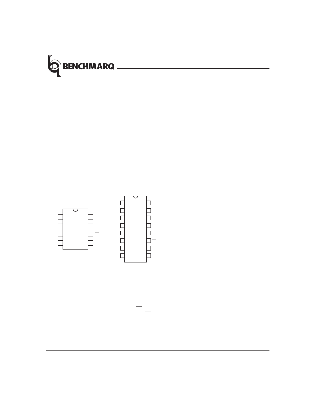
Pin Names
V
OUT
Supply output
BC
1
—BC
2
3-volt primary backup cell inputs
THS Threshold select input
CE chip-enable active low input
CE
CON
Conditioned chip-enable output
V
CC
+5-volt supply input
V
SS
Ground
NC No Connect
Functional Description
Pin Connections
An external CMOS static RAM can be battery-backed
using the V
OUT
and the conditioned chip-enable output
pin from the bq2201. As V
CC
slews down during a power
failure, the conditioned chip-enable output CE
CON
is
forced inactive independent of the chip-enable input CE.
This activity unconditionally write-protects external
SRAM as V
CC
falls to an out-of-tolerance threshold V
PFD
.
V
PFD
is selected by the threshold select input pin, THS.
If THS is tied to V
SS
, power-fail detection occurs at 4.62V
typical for 5% supply operation. If THS is tied to V
CC
,
power-fail detection occurs at 4.37V typical for 10% sup-
ply operation. The THS pin must be tied to V
SS
or V
CC
for
proper operation.
If a memory access is in process during power-fail detec-
tion, that memory cycle continues to completion before the
memory is write-protected. If the memory cycle is not ter-
minated within time t
WPT
, the CE
CON
output is uncondi-
tionally driven high, write-protecting the memory.
1
PN220101.eps
8-Pin Narrow DIP or SOIC
2
3
4
8
7
6
5
V
CC
BC
1
CE
CON
CE
V
OUT
BC
2
THS
V
SS
1
PN2201E.eps
16-Pin SOIC
2
3
4
5
6
7
8
16
15
14
13
12
11
10
9
NC
V
CC
NC
BC
1
NC
CE
CON
NC
CE
NC
V
OUT
NC
BC
2
NC
THS
NC
V
SS


