ADM485E/ADM487E/ADM1487E
Rev. 0 | Page 7 of 16
PIN CONFIGURATION AND FUNCTION DESCRIPTIONS
ADM485E/
ADM487E/
ADM1487E
TOP VIEW
(Not to Scale)
RO
1
RE
2
DE
3
DI
4
V
CC
8
B
7
A
6
GND
5
06356-002
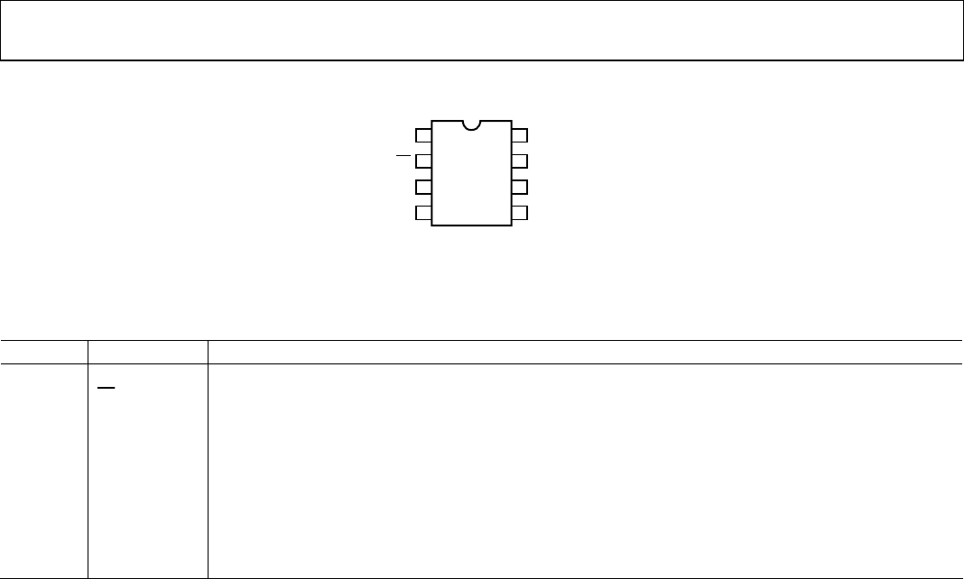
Figure 2. Pin Configuration
Table 6. Pin Function Descriptions
Pin No. Mnemonic Description
1 RO Receiver Output. When enabled, if A > B by 200 mV, then RO = high. If A < B by 200 mV, then RO = low.
2
RE
Receiver Output Enable. A low level enables the RO; a high level places it in a high impedance state.
3 DE
Driver Output Enable. A high level enables the driver differential outputs, Pin A and Pin B; a low level places it
in a high impedance state.
4 DI
Driver Input. When the driver is enabled, a Logic L = low on DI forces A low and B high; a Logic H = high on DI
forces Pin A high and Pin B low.
5 GND Ground Connection (0 V).
6 A Noninverting Receiver Input A/Driver Output A.
7 B Inverting Receiver Input B/Driver Output B.
8 V
CC
Power Supply (5 V ± 5%).


