Closed Dec 25th-26th
800-300-1968
We Stock Hard to Find Parts
My Account
|
My Orders
|
My Cart
Questions?
(800) 300-1968
Register
(current)
My Account
(current)
My Orders
(current)
My Cart
(current)
Categories
(current)
Manufacturers
Request a Quote
Sell Your Excess
Consignment
Quality Assurance
ADM485AN
Part #
ADM485AN
Description
LINE TRNSCVR 1TR 1TX 1RX 8PDIP - Rail/Tube
Category
IC
Availability
Out of Stock
Qty
0
Qty
Price
1 +
$3.36494
Related Items
Analog Devices
IC
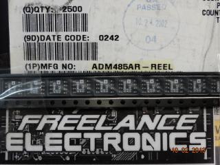
ADM485AR-REEL
$2.01101
Analog Devices
IC
ADM485JR
$1.05512
Texas Instruments
IC
ADM487EARZ
$0.79170
Analog Devices
IC
ADM489AR
$5.80945
Fairchild Semiconductor
IC
008-25424
$11.58351
Harris Corporation
IC
01-6945-9