Closed Dec 25th-26th
800-300-1968
We Stock Hard to Find Parts
My Account
|
My Orders
|
My Cart
Questions?
(800) 300-1968
Register
(current)
My Account
(current)
My Orders
(current)
My Cart
(current)
Categories
(current)
Manufacturers
Request a Quote
Sell Your Excess
Consignment
Quality Assurance
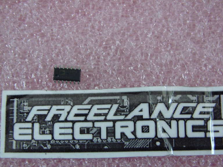
AD8608AR
Part #
AD8608AR
Description
OP Amp Quad GP R-R I/O 5.5V 14-Pin SOIC N - Rail/Tube
Category
IC
Availability
Out of Stock
Qty
0
Qty
Price
1 +
$2.63000
Related Items
Analog Devices
IC
AD8601ART
$2.36850
Analog Devices
IC
AD8605ART
$17.85262
Analog Devices
IC
AD8605ART-REEL
$0.89493
Analog Devices
IC
AD8606AR
$1.67251
AD / PMI
IC
AD860CA
Fairchild Semiconductor
IC
008-25424
$11.58351