Closed Dec 25th-26th
800-300-1968
We Stock Hard to Find Parts
My Account
|
My Orders
|
My Cart
Questions?
(800) 300-1968
Register
(current)
My Account
(current)
My Orders
(current)
My Cart
(current)
Categories
(current)
Manufacturers
Request a Quote
Sell Your Excess
Consignment
Quality Assurance
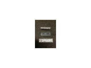
AD7541AKN
Part #
AD7541AKN
Description
IC DAC 12BIT MULTIPLYING 18-DIP
Category
IC
Availability
Out of Stock
Qty
0
Qty
Price
1 +
$9.78225
Related Items
Analog Devices
IC
AD7541AD/883B
$53.28527
Harris Corporation
IC
AD7541KN
$10.65997
Analog Devices
IC
AD7541SQ/883B
$121.75876
INTERSIL
IC
AD7541TD/883B
$21.50608
Analog Devices
IC
AD7542GBD
$82.93234
Analog Devices
IC
AD7544GKN
$33.17291